June 15, 2026
At 1:00 AM, the PM group chat pings with a client's LINE message: "Mass production starts next month, the unit price needs to drop by another 8 cents, or the order might shift to Vietnam." The first ones woken up for a meeting are always Procurement and the Assembly Plant PMs. When the call connects, the assembly plant contact is polite, but the answer is almost always the same: "The design is locked in; I really can't squeeze out any more on my end." This script plays out in every hardware company multiple times a year. The problem is—the play was cast wrong from the very beginning.
There is a repeatedly verified concept in the industry:
Nearly 70% to 80% of a PCBA's cost is locked in the moment the circuit design is completed.
Once the Gerbers are sent, the BOM enters the procurement system, and the components hit the SMT line, the remaining negotiation room is so small that even the best procurement teams can only squeeze out 2% to 3%. And this 3% is often bought at the expense of payment terms, lead times, or even quality.
The real cost battlefield isn’t on the assembly plant’s quotation sheet; it’s the moment the design engineer opens their EDA software.
Below are four entry points that ODM plants, hardware startups, and IPC manufacturers should immediately review. Each comes with concrete numbers, and each can be practically implemented before your next shipment.
Many engineers feel that component selection is procurement’s job. In reality, every line on the BOM is a promise personally written by the design engineer.
Mainstream SMD packages like 0402, 0603, and 0805 have the highest circulation volume globally. Prioritising them instantly grants three benefits:
 Conversely, if you force the use of niche packages to make a design “more refined”, or choose 0.1% tolerance resistors for “engineering rigor”, it might look strict on paper, but you are effectively hardcoding unnecessary costs into mass production.
Important Note: RoHS compliance must be unified from the very beginning. Mixing RoHS and non‑RoHS components forces a hybrid assembly process, and this action alone can double your unit price.
Many assume yield is the SMT plant’s problem. This is a mistake. The root of yield issues almost entirely resides in the design files.
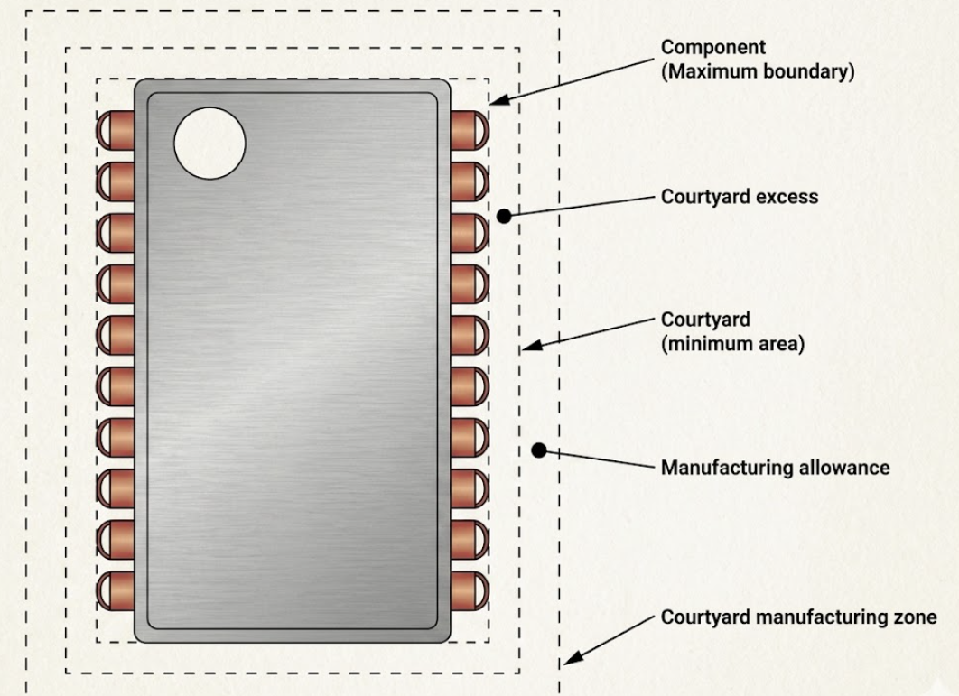
Crowding components together inevitably leads to solder bridging, false AOI rejects, and X‑ray bottlenecks – each of which is a yield killer. Ultimately, this reflects on your billing statements as bloody “rework fees” and “special acceptance fees” .
These are not textbook regulations; they are the minimum thresholds to ensure the SMT plant doesn’t have to resort to special acceptance, custom fixtures, or manual touch‑ups.
During reflow and backend processes, the centre of the circuit board experiences the highest stress from bowing and twisting. If you place BGAs, large ceramic capacitors, or sensitive packages in the centre of the board, the probability of solder cracking and cold joints during mass production will drastically increase.
Spread out sensitive components, leave clearance at the edges, and reserve the centre for stable components. Executing these three things alone will improve yield, directly driving down costs and boosting gross margins.
SMT lines have long been fully automated, yet many design files are still stuck in a “manual‑friendly” mindset. It’s 2026, and this is like writing a web page that can only run on IE6. The equipment is new, but the underlying logic is outdated.
Every small detail saves the pick‑and‑place robotic arm travel distance and calibration time. Accumulated, this frequently creates a 10% to 20% assembly time difference per board. For mass production runs of tens or hundreds of thousands of boards, this 10‑20% isn’t just a percentage – it’s six figures of real money.
Many design engineers treat DFT (Design for Testing) as a task to “quickly patch in right before mass production after the layout is finished”. This is a misunderstanding that will slowly bleed you dry.
If DFT is designed well, boards can run diagnostics the moment they roll off the assembly line. If DFT is poorly designed, every defective board requires a teardown. And the cost of tearing down and starting over is always ten times more expensive than drawing a few extra test points at the start.
Reading up to this point, most engineers will think: “I already know all of this.”
However, in practice, nearly half of the Gerber files we see step on at least two or three of the landmines mentioned above. The reasons usually boil down to three things:
None of these are issues of engineering capability; they are issues of process design.
The competition in PCBA is no longer operating on the level of “which assembly plant quotes the lowest”.
The real differentiator is whether the design team is willing to spend an extra 30 minutes running a complete check on the BOM, layout, silkscreen, and test points before sending out the Gerbers.
What those 30 minutes save isn’t just material costs, but:
Cost control is not an after‑the‑fact income statement; it is a series of multiple‑choice questions made right at the design desk.
The next time a client calls demanding a price cut, remember: go back and look at your EDA software first, instead of immediately calling your assembly plant.