June 28, 2026
In application scenarios requiring frequent insertion and extraction—such as server backplanes, modular instruments, and PCIe interface cards—the row of golden contacts on the edge of the board plays a critical role in determining the reliability of the entire system. These are what the industry commonly refers to as "Gold Fingers." For engineers responsible for PCB design, procurement, or quality control, gold fingers are by no means as simple as "just adding a layer of gold." From the thickness of the nickel-gold stack-up and the tolerance of the bevel angle to the subsequent wear-resistance cycle testing, every link directly impacts the product's service life in the field. This article breaks down the design logic, manufacturing details, and selection criteria for gold fingers from a practical perspective.
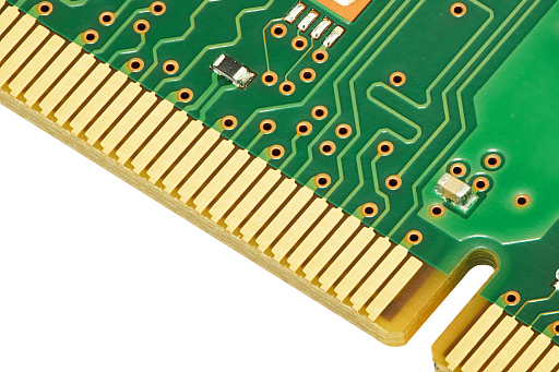
Many engineers encountering gold fingers for the first time mistakenly believe they belong to the same category as ENIG (Electroless Nickel Immersion Gold) or OSP, with the only difference being that “the gold is thicker.” In fact, these two solve entirely different engineering problems:
If you use ENIG for gold fingers, it might look “golden,” but after fewer than a few hundred insertions, the nickel layer will wear through, the substrate will oxidise, and the contact resistance will spike. This is why the “Hard Gold” electrolytic plating process must be used.
The standard structure of a gold finger is:
The key to this combination is that the ability of hard gold to resist friction and fretting corrosion is an order of magnitude higher than that of tin‑lead or soft gold (pure gold). This is the fundamental reason it is capable of handling hot‑swap and field‑repairable systems.
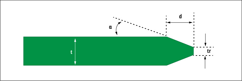
Many design engineers meticulously mark the length and spacing of gold fingers on their Gerber files but overlook the specifications for board edge beveling. However, during actual assembly, the bevel is often the detail that determines success or failure.
Mainstream bevel angles in the industry fall between 20°–45°, with 30° and 45° being the most common. During the design phase, it is recommended to confirm the following parameters with the board manufacturer before prototyping:
The front‑end manufacturing process for gold fingers is identical to standard PCBs (image transfer, etching, lamination, drilling). The real differences occur in the back‑end. Typical steps include:
It is worth noting that hard gold plating is a selective plating process applied only to the gold finger area. This is why the design must clearly define the plating bar, lead‑in lines, and the method for removing them after mass production.
When inspecting gold fingers, the key areas of focus for OQC and clients include:
The unit cost of a hard gold surface finish is significantly higher than ENIG or OSP, but it remains the most cost‑effective choice in the following scenarios:
If you shift your focus from “BOM Cost” to “Total Cost of Ownership (TCO)” , you will find that the RMA labour, customer claim compensation, and downtime losses saved by using a hard gold board often far exceed the slight price difference in electroplating.
The following IPC standards are the most frequently cited references during quotation, manufacturing, and acceptance of gold finger PCBs:
In practice, many clients also add gold thickness specifications (e.g., 30 µ" / 0.76 µm or more) and insertion cycle requirements in the PO or drawing notes. It is highly recommended to establish two‑way confirmation with the board manufacturer during the design phase to avoid discovering that the process capability cannot meet the specifications during mass production.
The biggest difference lies in the process and application. Hard gold uses electrolytic plating and contains trace amounts of cobalt or nickel to harden it, specifically designed to withstand mechanical friction. ENIG is an electroless immersion deposition where the gold layer is extremely thin (≈ 0.05 µm) and serves solely for soldering wettability. If you use ENIG for gold fingers, the nickel layer will wear through after a few hundred insertions.
It depends on the required number of insertion cycles:
| Application Level | Recommended Gold Thickness | Insertion Cycles Reference | | :--- | :--- | :--- | | General Consumer | ≥ 0.5 µm | Hundreds | | Industrial / Hot‑Swap | 0.76–1.27 µm (30–50 µ") | Thousands | | Military / Medical | > 1.5 µm | Tens of thousands |
It is advisable to specify the expected insertion cycles in your spec sheet during the RFQ phase.
Theoretically yes, but practically it comes at a cost. Inserting a board without a bevel concentrates severe stress on the socket springs, which can scratch the receptacle's plating at best, and cause poor contact at worst. In the long run, beveled boards simultaneously maintain the contact quality and lifespan of both the receptacle and the male board, which is the fundamental reason the industry universally demands edge beveling.
Gold fingers may look like just a row of golden contacts, but from the microstructure of hard gold plating to the geometric tolerances of edge beveling, every detail is an accumulation of long‑term reliability.
For PCB design and procurement teams, rather than holding the board manufacturer accountable after mass production issues arise, it is better to clearly communicate specifications with the manufacturer's technical window during the design phase. This is the core reason why eCloud has always emphasised “face‑to‑face DFM and stack‑up discussions.”
If you have a design project involving gold fingers, or if you have stricter requirements for custom gold plating thickness and insertion cycles, you are welcome to reach out to our local service window in Taoyuan for further discussion. Our engineering team will assist you in translating your specifications into practical manufacturing capabilities.
