June 29, 2026
While the market focuses on NVIDIA GPU computing power and HBM capacity, few have noticed that the value of PCBs in an entire AI server rack has skyrocketed from approximately $25,000 in the GB200 generation to an estimated $160,000 or more in the Rubin Ultra generation. This sixfold leap in value over three years reflects a structural upgrade forced upon the entire PCB industry. This article breaks down this industry-reshaping technological revolution layer by layer, from signal physics and materials science to manufacturing limits.
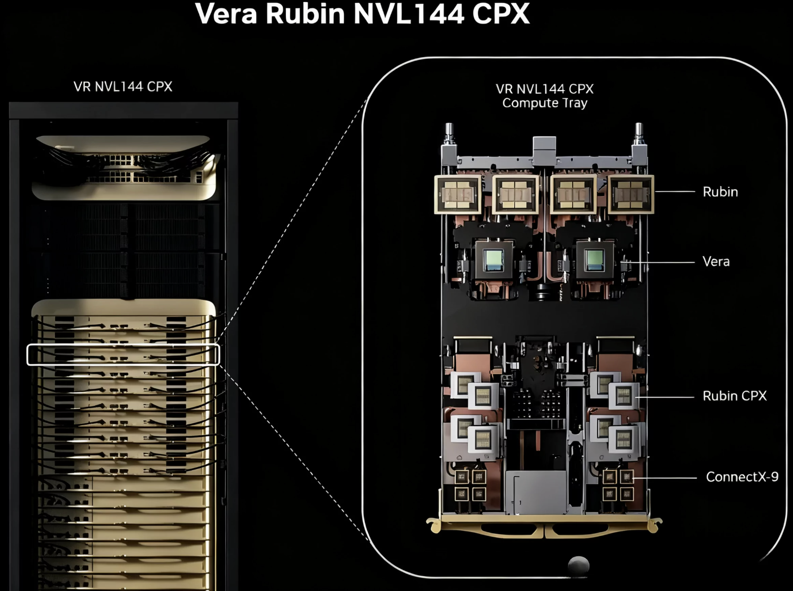
In the past, when designing servers, we were accustomed to viewing the entire system as a motherboard plus peripheral accessories. But stepping into the Compute Tray of the Rubin generation, you will find at least five types of PCBs operating synchronously:
Every board's layer count, materials, and manufacturing processes are being rewritten. Most crucially: the Midplane is an entirely new PCB category created out of thin air – it completely did not exist in the GB200 and GB300 generations.
Many people think increasing layer counts is something engineers do “just because they want to.” In reality, this is a strict constraint driven by high‑speed signal physics.
The signal rate for NVLink 5 is 112G PAM4, upgrading to 224G PAM4 in NVLink 6, and reaching 448G SerDes in Rubin Ultra.
| PCB Type | GB200 | GB300 | Rubin NVL144 | Rubin Ultra | | :--- | :--- | :--- | :--- | :--- | | HPM Motherboard | 22 Layers | 22+OAM | 24 Layers | 26 Layers | | NVSwitch | 24 Layers | 26 Layers | 32 Layers | 40+ Layers | | Midplane | None | None | 44 Layers | 78 Layers | | CX9 HDI Card | None | None | 22 Layers | 24 Layers |
The increase in motherboard layers is relatively mild, but NVSwitch sees a massive jump, and the Midplane goes from zero straight to 78 layers – a magnitude of evolution the PCB industry has not seen in the past decade.
The “blood” of a PCB is the Copper Clad Laminate (CCL). Panasonic's Megtron series from M4 to M9 is essentially a materials science race involving the dielectric constant (Dk) and dissipation factor (Df):
The difficulty of stepping from M8 to M9 is not about tweaking a formula; it is a simultaneous generational shift across three major materials: the resin system, fibreglass cloth, and copper foil.
If any of these three materials fails to meet the standard, the entire board must be scrapped. Yields plummet from 85% in the M7 generation to about 50% for M9. This is why only three companies globally – Panasonic, Showa Denko, and Isola – can stably mass‑produce M9 CCL.
CCL volume is comprised of about 40% fibreglass cloth, yet it almost entirely dictates the overall Dk performance of the board. The evolutionary logic of the five generations of fibreglass cloth is as follows:
Japan's Nittobo alone commands over 90% of the high‑end fibreglass cloth market share. Prices were already hiked by 20% in August 2025, and the market expects further increases in the first half of 2026. For Taiwanese PCB manufacturers, pricing power for upstream materials is almost entirely in the hands of Japanese companies – a reality they must face when planning high‑end product lines.
When discussing why 224G signals must be paired with copper foil of HVLP4 grade or higher, we must return to a fundamental physics concept: the Skin Effect.
The five‑generation evolution of HVLP copper foil is essentially a challenge against manufacturing limits, grinding surface roughness (Rz) all the way down from 6‑10 µm to 0.3‑0.5 µm:
Global manufacturers capable of mass‑producing HVLP4 are highly concentrated among Japanese (Mitsui, JX, Furukawa, Fukuda) and Korean (ILJIN, LOTTE) companies. Other regions in Asia are still playing catch‑up.
HDI designs use “stages” to indicate complexity:
Adding one stage means facing several new hurdles:
This is why manufacturers capable of producing 32+ layer Ultra‑Low‑Loss PCBs and 5/6‑stage HDIs can be counted on one hand globally.

GB200 and GB300 used Cable Cartridges to connect GPUs and switch chips. While theoretically a high‑speed solution, in reality, it became the biggest bottleneck for mass production:
Rubin switched to a PCB Midplane to directly solve all these problems:
From the 44‑layer Midplane in the Rubin NVL144 to the 78‑layer rack‑level Midplane in the Rubin Ultra Kyber, this board is rapidly becoming the single category with the highest value proportion in the entire rack's PCB – estimated to account for 38% of the Rubin Ultra rack's total PCB value.
The three‑year leap from GB200 to Rubin Ultra is essentially not just a “PCB price hike,” but a forced upgrade of the entire industry chain to aerospace‑grade materials. For the Taiwanese PCB supply chain, there are several key observations worth reviewing repeatedly in engineering and business strategies:
The AI computing arms race is rewriting the competitive landscape of the PCB industry for the next decade. From signal physics and materials science to manufacturing limits, every variable is redefining what constitutes a “high‑end board.” For all R&D engineers and decision‑makers, understanding the physical roots of these changes is more important than chasing trending buzzwords – because the next wave of order allocations will be officially revealed in the first half of 2026.
