August 31, 2026
An electric vehicle combines a high-voltage power system operating at hundreds of volts, currents ranging from tens to hundreds of amperes, low-noise sensing, high-speed in-vehicle communications, and millimeter-wave radar. Although all these circuits operate in the same vehicle, they place very different demands on their PCBs. There is therefore no single answer to the question, “Which PCB should an EV use?” A battery-management system requires accurate measurement and high-voltage isolation. A traction inverter emphasizes high-current switching and thermal management. ADAS electronics require signal integrity and high-density interconnects. The correct approach is to understand each subsystem’s electrical, thermal, and mechanical loads before selecting the laminate, copper weight, stackup, and manufacturing process.
A battery‑management system monitors cell voltage and temperature, measures current, estimates state of charge, balances cells, controls contactors, and manages fault protection.
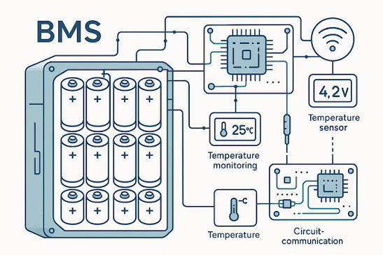 A BMS may combine low‑level analog measurements, a high‑voltage battery stack, and vehicle communications. Without clear separation among high‑voltage, low‑voltage, analog, digital, and communication areas, switching noise can enter measurement paths and affect voltage or current readings.
The design review should address:
A BMS does not necessarily require heavy copper throughout the board. The high‑current, contactor‑control, and current‑measurement sections may need a different conductor and thermal strategy from the low‑current monitoring circuits.
A traction inverter converts battery DC power into AC power for the motor. High‑speed switching by SiC MOSFETs or IGBTs produces high dv/dt, high di/dt, common‑mode noise, and localised thermal loads.
The primary power path is often handled by power modules, busbars, direct‑bonded copper substrates, or other dedicated structures. The control PCB manages gate driving, current and temperature sensing, protection, and communications. A high‑power application does not automatically mean that all current should be routed through conventional PCB copper.
Gate‑driver board design should consider:
Ignoring parasitic elements can produce false turn‑on, overshoot, ringing, or EMI even when the schematic is functionally correct.
An onboard charger converts external AC power into regulated DC power for the battery. A DC‑DC converter transfers energy between the high‑voltage battery and the 12 V or 48 V system.
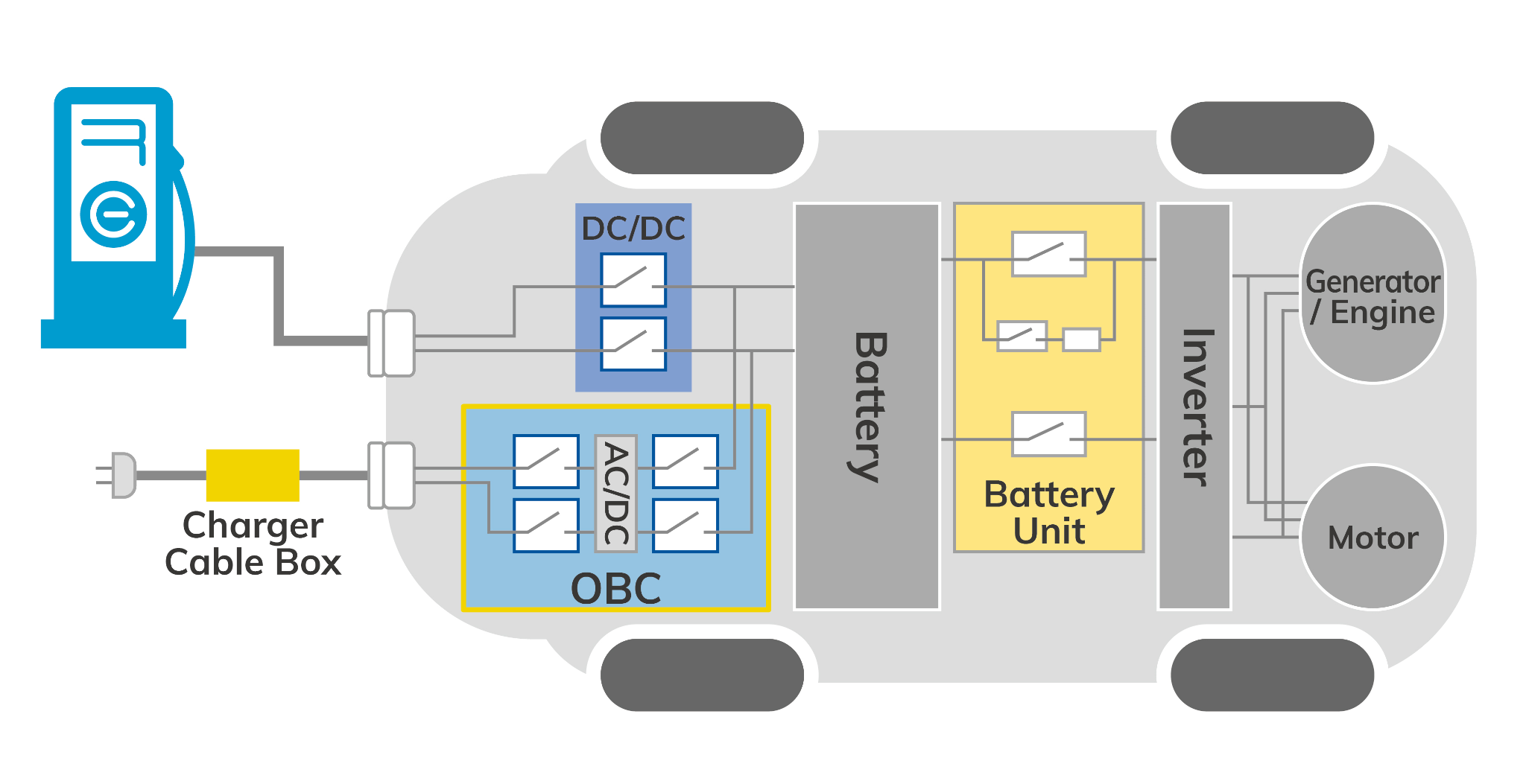 These products combine power‑factor correction, transformers or inductors, high‑frequency switching devices, rectification, and control circuitry. Their PCBs must address:
Creepage and clearance cannot be selected from operating voltage alone. Material group, pollution degree, altitude, transient voltage, conformal coating, and applicable safety requirements can all change the required distances.
A power distribution unit manages high‑voltage distribution, protection, pre‑charge, and contactor control. Some designs use heavy‑copper PCBs, but as current increases, busbars, copper inlays, or hybrid power boards may be more appropriate than simply increasing copper thickness across the entire board.
Thicker copper improves current capacity and heat spreading, but creates new DFM tradeoffs:
Copper thickness should therefore be determined from the current waveform, acceptable temperature rise, heat‑spreading conditions, ambient temperature, and fault duration—not from current alone.
Cameras, radar, LiDAR, central computers, and network gateways are driven less by high current than by high data rates, low latency, and electromagnetic compatibility.
 These modules may use multilayer, HDI, flex, rigid‑flex, or low‑loss materials to support Automotive Ethernet, SerDes, MIPI, LVDS, CAN FD, and RF signals.
Key design considerations include:
Not every ADAS board needs PTFE. Material selection should be based on operating frequency, insertion‑loss budget, thermal stability, manufacturability, and cost—not merely on a “high‑frequency” label.
Flex and rigid‑flex circuits can fit narrow or irregular spaces while reducing selected wire harnesses and connectors. They are commonly considered for battery modules, cameras, displays, and sensor interconnects.
A flexible structure, however, cannot be bent without limits. Confirm:
Without early coordination among mechanical, PCB, and manufacturing teams, the flex‑to‑rigid transition can become a location for copper cracking, delamination, or concentrated stress.
| EV subsystem | Main engineering challenge | Common PCB or substrate direction | | :--- | :--- | :--- | | BMS | Precision measurement, high‑voltage isolation, and communications | Multilayer boards, localised high‑current design, and flex interconnects | | Traction inverter | High dv/dt, gate loops, and heat | Control PCB, IMS, DBC, or hybrid power structures | | OBC/DC‑DC | High voltage, switching, thermal management, and EMI | High‑Tg multilayer, heavy copper, IMS, or hybrid construction | | PDU | High‑current distribution and fault protection | Heavy copper, busbars, copper inlays, or power‑combination boards | | ADAS | High‑speed signalling, density, and latency | HDI, low‑loss multilayer, and RF materials | | Cameras/sensors | Miniaturisation, vibration, and packaging | HDI, flex, and rigid‑flex | | Vehicle communications | Impedance, EMC, and interface integrity | Controlled‑impedance multilayer and localised low‑loss materials |
These categories are starting points, not fixed answers. A single subsystem may contain separate control, power, sensing, and interconnect boards.
Before selecting the material and stackup, the circuit, layout, mechanical, thermal, functional‑safety, and manufacturing teams should jointly confirm:
IPC‑A‑610 may form part of the electronic‑assembly acceptance requirements. AEC‑Q100 primarily addresses stress‑test qualification for integrated circuits. ISO 26262 covers the functional‑safety lifecycle of road vehicles. They apply to different subjects and should not be treated as interchangeable proof that an entire PCB is “automotive qualified.”
The challenge of EV PCBs comes from the coexistence of high voltage, high current, high‑speed signalling, thermal cycling, vibration, and long‑term reliability requirements. However, every board does not need every advanced technology.
A sound architecture gives the BMS, inverter, OBC, PDU, ADAS, and communication modules the materials and structures appropriate to their individual risks. Isolation, thermal, signal, mechanical, and manufacturing conditions should then be cross‑checked early in development.
For automotive projects involving high voltage, high current, HDI, rigid‑flex, or low‑loss materials, the eCloud engineering team can review stackups, laminate choices, isolation regions, and DFM risks before prototyping, helping align design requirements with practical manufacturing capability.
