September 1, 2026
A conventional USB or IP camera primarily captures images and transfers them to a host or server. An Edge AI camera must also perform image preprocessing, AI inference, event decisions, and communications locally. Once computation moves into the camera, PCB design involves much more than integrating an image sensor and a network interface. A single Edge AI camera board may combine a CMOS image sensor, SoC or NPU, DDR memory, storage, Ethernet, PoE power, USB, wireless connectivity, audio, and motor control. When these functions are compressed into a small enclosure, signal integrity, power integrity, thermal management, EMI, and manufacturing risk become closely interconnected.
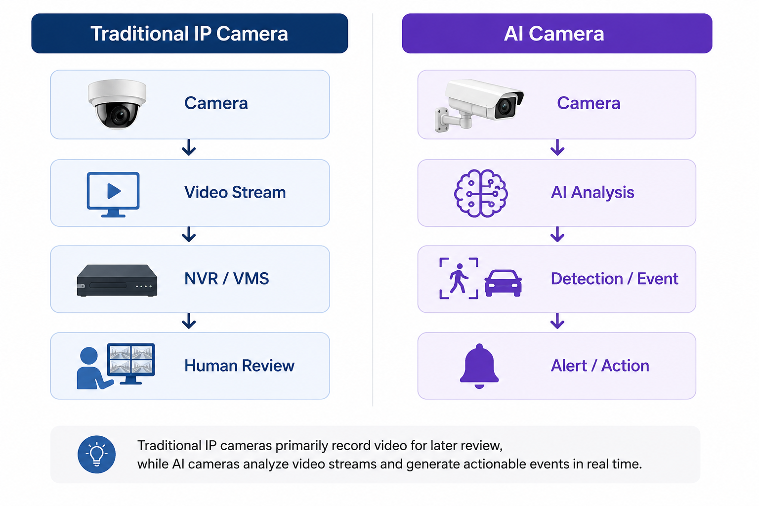 Edge AI vision systems commonly use one of two architectures:
| Architecture | Characteristic | Main PCB challenge | | :--- | :--- | :--- | | Integrated AI camera | Sensor and computing board reside in one device | Space, heat, noise, and optical placement constrain one another | | Camera plus Edge AI box | Cameras capture images while an external unit performs processing | High‑speed transport, connectors, cables, and multi‑camera synchronisation |
An integrated design shortens the image‑data path and reduces device count, but places the processor's heat source closer to the sensor. An inadequate thermal path can increase sensor temperature and image noise. Thermal expansion among the lens mount, PCB, and enclosure may also affect alignment.
 An AI‑box architecture provides more room for cooling and computing resources, but introduces video‑bandwidth, latency, cable‑loss, and connector‑reliability concerns.
Before choosing the architecture, define the number of video streams, resolution, frame rate, inference‑latency target, and whether raw images are permitted to leave the camera.
CMOS sensors commonly connect to the main processor through MIPI CSI‑2. Although this interface is generally short, its high data rate and proximity to clocks and power circuits can still create impedance discontinuities, crosstalk, and broken return paths.
The layout should:
In a modular sensor design, checking only the main‑board traces is insufficient. Connectors, flex circuits, and module boards form the complete channel, and discontinuities in any section may affect image stability.
AI inference repeatedly accesses images and model data, making the SoC‑to‑DDR region one of the densest and most sensitive sections of the board. If component placement is completed before the stackup is defined, the design may lack sufficient BGA breakout layers or suitable reference planes for data, address, and clock signals.
Before layout, confirm:
DDR constraints must come from the selected SoC and memory vendors' design documentation. Length and matching values from another platform should not be copied into a new design.
An AI SoC's load changes rapidly as different parts of the model execute. Even with moderate average power, fast current transients can cause core‑voltage droop, increased noise, or system resets.
The power design must address more than regulator current rating:
Noise from the SoC, DDR, or DC‑DC converters entering the sensor's analog rails may create fixed‑pattern noise, banding, or degraded low‑light performance. Sensor supplies and grounds should follow the device vendor's filtering and partitioning guidance.
Power over Ethernet allows an AI camera to receive data and power through one cable, simplifying field installation. The PCB must, however, handle network signals, common‑mode noise, isolation, surge events, and power conversion simultaneously.
The PoE region should be reviewed for:
USB, GPIO, motors, microphones, and wireless antennas can also become paths for ESD or noise coupling. Protection devices should be placed near the energy‑entry point rather than only where they are convenient on the schematic.
An Edge AI camera has limited enclosure space, while the SoC, DDR, PoE supply, and image sensor may all be concentrated in one area. Addressing only the SoC junction temperature can still leave image quality, component aging, or power derating as system‑level failure mechanisms.
Evaluate the complete thermal path:
junction → package → PCB or thermal interface → heat sink or enclosure → ambient
PCB techniques may include thermal vias, larger copper areas, internal spreading planes, and thermal pads connected to the enclosure. Via location, diameter, filling method, and solder‑mask opening affect manufacturing and assembly and should be reviewed accordingly.
The location of the heat source relative to the optics also matters. Long‑term heating of the sensor or lens mount by the SoC or PoE supply may affect dark current, focus stability, or sealing‑material life.
Replaceable sensor, lens, communications, or computing modules can shorten platform development, but every board‑to‑board connector introduces new signal, power, mechanical, and supply‑chain risks.
A module interface should define:
For outdoor or industrial use, include moisture, dust, corrosion, temperature cycling, and connector fretting in the reliability plan.
| Area | What to confirm | | :--- | :--- | | System architecture | Stream count, resolution, frame rate, latency, and local‑storage requirements | | MIPI/video | Impedance, length, vias, reference planes, and connector channel | | DDR | Stackup, topology, matching, BGA breakout, and vendor constraints | | Power | Transients, sequencing, decoupling, high‑di/dt loops, and plane neck‑downs | | PoE/network | Isolation, protection, differential pairs, magnetics, and discharge paths | | Thermal | Complete heat paths for the SoC, sensor, DDR, and power devices | | EMI/ESD | Switching nodes, external interfaces, chassis grounding, and sensitive‑area partitioning | | Optics/mechanics | Lens centre, sensor flatness, screw stress, and tolerance stack | | Manufacturing | HDI structure, microvias, via‑in‑pad, board thickness, and assembly capability | | Testing | Power test points, image test, networking, programming, and thermal verification |
Moving AI inference into the camera requires more than adding an NPU. The image sensor, DDR, power system, networking, PoE, heat sink, and optical mechanics must operate together within a limited volume.
Successful Edge AI camera PCBs are generally not created by solving each issue late in layout. Stackup, power demand, heat flow, optical placement, and manufacturing capability should be reviewed together during component selection.
For projects involving MIPI CSI‑2, DDR, PoE, HDI, or compact thermal design, the eCloud engineering team can review the stackup, materials, microvia arrangement, and DFM risks before prototyping, helping align high‑speed interfaces, thermal requirements, and manufacturing conditions before fabrication.
