September 6, 2026
OpenAI’s demonstration of GPT-6 Astra operating KiCad to design PCBs highlights a significant leap in automation, yet successful hardware development still requires overcoming critical practical challenges
OpenAI claims GPT-6 Astra can make PCB boards.
That statement has triggered intense discussion across engineering communities. More importantly, this is not simply an AI answering circuit-design questions. The demonstration shows AI operating KiCad directly: reading an existing schematic, placing components, and routing copper connections on a PCB.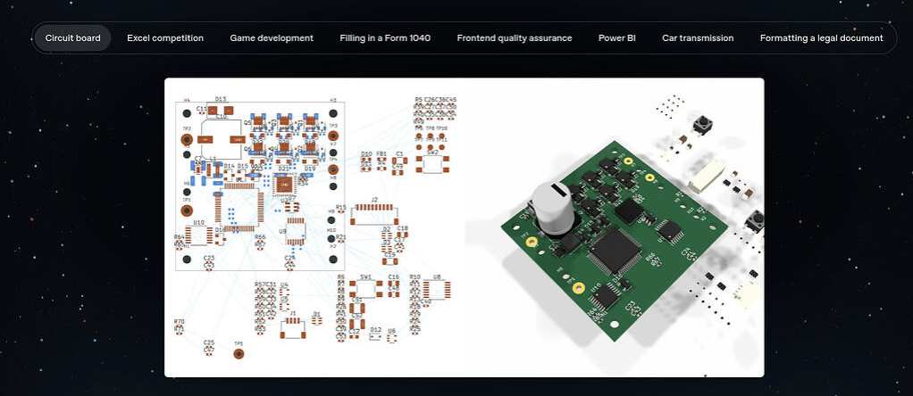
For a general audience, this may look like another impressive AI demonstration. For R&D engineers, PCB layout specialists, and hardware project managers, the implications are more significant. PCB layout has long been considered difficult to automate completely because connectivity is only the baseline requirement. Product performance often depends on conditions that are not fully represented in the schematic: power-loop geometry, return paths, decoupling placement, signal integrity, EMI, thermal behavior, mechanical restrictions, and the actual process capabilities of the PCB fabricator.
GPT-6 Astra can now turn a schematic into what appears to be a completed PCB layout. Does that mean AI has crossed the hardest barrier? The answer is nuanced: it represents a major step forward, but there is still a critical gap between completing a layout and taking responsibility for the design result.
Autorouting itself is not new. Once nets, trace widths, clearances, and layer assignments are configured, conventional autorouters can already search for possible routing paths. What makes the GPT-6 Astra demonstration more notable is its ability to connect multiple steps into a broader engineering task. AI can interpret instructions, operate an EDA tool, inspect the outcome, and continue modifying the design in response to errors.
In the future, engineers may describe design objectives instead of issuing every individual command:
AI is therefore moving from an engineering question-and-answer assistant toward an agent capable of modifying real design files. However, the ability to operate a tool is not the same as understanding the product. The hardest part of PCB layout is often not drawing a trace, but determining why that trace must be routed in a particular way.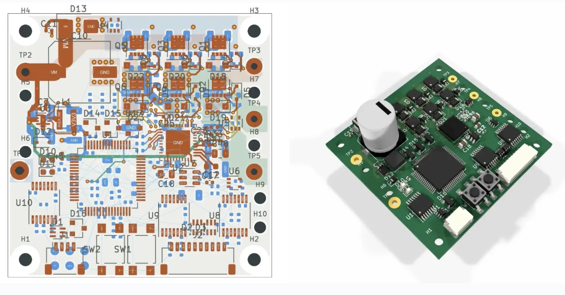
AI performs well when objectives are explicit, measurable, and supported by feedback. It can attempt to complete all nets, reduce unconnected items, avoid clearance violations, and pass DRC. The problem is that many conditions affecting product success do not exist in the schematic. For example:
If these conditions have not been converted into design rules or explicit instructions, AI can only infer them from the available information. It may produce a board that is fully connected, visually organized, and free of obvious DRC violations while still leaving risks in power integrity, signal integrity, thermal behavior, EMI, or manufacturability.
The AI may not be completing the task incorrectly. More often, it is completing an incompletely defined task extremely well.
This is the most important expectation that R&D teams and PMs must establish before introducing AI PCB design.
Electrical Rules Check, or ERC, primarily identifies structural issues such as unconnected pins and power-pin conflicts. Design Rules Check, or DRC, evaluates the layout using configured trace widths, clearances, hole sizes, net classes, and other constraints. Both are essential, but they can only check rules that have already been defined.
If the fabricator’s process capabilities have not been entered correctly, the stackup and impedance have not been confirmed, special nets do not have dedicated constraints, or warnings have been ignored, a zero-error DRC result only means the design passed the current configuration. It does not mean the design is ready for production. DRC also does not fully determine whether:
An AI-generated design cannot be approved simply because no red error markers remain on the screen.
At this stage, dividing the process into small, verifiable tasks is more practical than asking AI to complete an entire PCB in one attempt.
| Suitable for early AI adoption | Still requires engineering review or approval | | :--- | :--- | | Generate preliminary placement concepts | Placement of critical components and functional blocks | | Route general, lower-risk signals | Power, high-speed, RF, analog, and high-current regions | | Compare schematic, BOM, and layout information | Component choice, footprints, polarity, and pin mapping | | Organize ERC, DRC, and review actions | Whether DRC rules reflect the actual design requirements | | Generate alternatives for engineering comparison | Stackup, impedance, thermal, EMC, and reliability | | Assist with output preparation | Final release of Gerber, drill, and assembly data |
The core principle is simple: AI may generate the design, but the engineering team must define the acceptance criteria. Without clear constraints, review gates, and ownership, AI will increase output speed without necessarily improving design quality.
The first effect of AI may not be the elimination of roles, but a change in what each role contributes to the project.
R&D: From Supplying a Schematic to Defining Complete Design Intent Beyond the schematic, R&D engineers will need to identify critical nets, current conditions, timing requirements, interface priorities, and expected failure risks more clearly. The more complete the input, the more reviewable the AI-generated result becomes.
Layout Engineering: From Routing Execution to Constraint and Risk Management General placement and repetitive routing may become increasingly automated. Power, return paths, high-speed design, thermal behavior, and EMC still require cross-domain judgment. Layout engineers will contribute more through constraint management and design approval.
Project Management: Do Not Confuse Layout Speed With Development Completion AI may reduce the time required to generate a first draft, but component verification, engineering review, DFM, prototyping, and bring-up do not disappear. If a PM sees a rapidly completed layout and compresses the remaining verification schedule, project risk may simply move into a later and more expensive stage.
A practical AI PCB design process should not end when the AI completes routing. It should form a closed loop:
With this loop in place, AI can help reduce the overall development cycle instead of merely accelerating drawing.
OpenAI claims GPT-6 Astra can make PCB boards—and based on the demonstrated tool-use capabilities, that statement is not entirely without merit. AI is beginning to place components, route connections, and modify PCB designs directly.
However, “making a PCB board” can describe very different levels of completion.
If the standard is an editable KiCad design with completed connectivity, AI has made clear progress. If the standard is a manufacturable and assemblable product that passes functional, thermal, EMC, and reliability validation, engineering and manufacturing reviews remain essential.
The real change introduced by GPT-6 Astra is not the immediate disappearance of R&D, PM, or layout engineering roles. It is the declining value of tool operation alone—and the rising importance of requirement definition, constraint development, risk identification, and result verification.
AI can accelerate PCB layout. The engineering team’s verification capability still determines whether the product is ready for release. Teams preparing to introduce AI PCB design should begin with design rules, review gates, and DFM processes rather than pursuing full automation immediately. eCloud can help clarify PCB requirements and DFM priorities from a practical manufacturing perspective, reducing the risk of discovering process issues only after the design has been completed.
