September 12, 2026
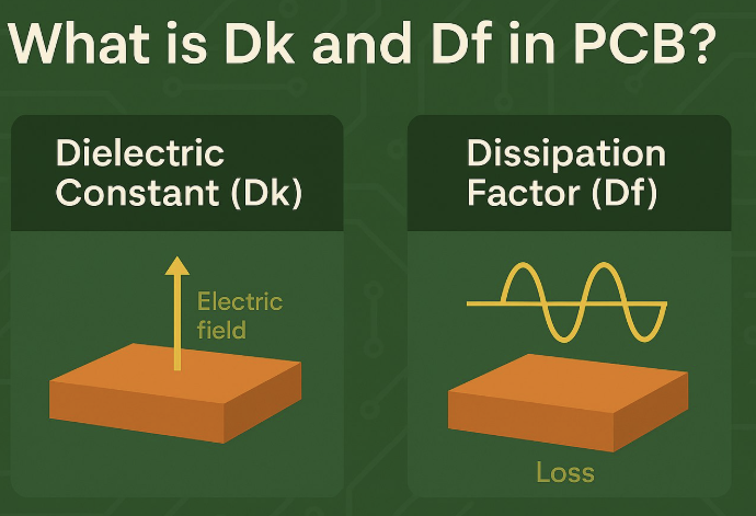
Two traces with identical geometry may exhibit different characteristic impedance, propagation delay, and resonant behavior when the PCB laminate is changed. The difference often comes not from the copper itself, but from the dielectric surrounding it. This material property is relative permittivity, commonly called dielectric constant or Dk in the PCB industry. Dk, however, is not a permanent identification number for a material. It can vary with frequency, temperature, moisture content, material orientation, and test method. The practical objective is therefore not to memorize the Dk of FR-4, water, or ceramic materials. Engineers need to understand where the value comes from and which value is appropriate for a particular design.
 Relative permittivity is the ratio between a material's absolute permittivity, ε, and the permittivity of vacuum, ε₀:
εᵣ = ε/ε₀
The value of ε₀ is approximately 8.854 × 10⁻¹² F/m, while the relative permittivity of vacuum is defined as 1. In engineering discussions, "dielectric constant" usually refers to the dimensionless relative permittivity εᵣ.
When a dielectric is exposed to an electric field, positive and negative charges within the material undergo a small relative displacement. The resulting polarization field partially opposes the applied field. For an ideal parallel-plate capacitor:
C = ε₀εᵣA/d
With the same geometry, a higher εᵣ produces a higher capacitance. This does not mean that a higher dielectric constant is inherently better; it only indicates a stronger polarization and electric-energy storage response.
An electric field slightly displaces the electron cloud relative to the nucleus. Electronic polarization exists in every dielectric and can respond at very high frequencies.
At optical frequencies, slower polarization mechanisms generally cannot follow the rapidly changing field. The response is therefore dominated by electronic polarization. Under applicable low-loss, nonmagnetic conditions, the relationship can be approximated as $n^2 \approx \varepsilon_r$. This does not mean that a material's Dk equals $n^2$ at every frequency.
In ionic crystals, positive and negative ions shift in opposite directions. The resulting contribution depends on ionic charge, bonding, lattice stiffness, and crystal structure. It cannot be reduced to a universal rule that stronger ionic bonding always produces a higher Dk.
Many metal oxides have a higher Dk than common polymers, but crystal phase, defects, and measurement frequency can still produce substantial variation.
Molecules with permanent dipole moments tend to align with an applied field. This mechanism helps give water a relative permittivity of approximately 78 under room-temperature, low-frequency conditions.
As temperature rises, thermal motion interferes with dipole alignment. NIST measurements confirm that the static permittivity of liquid water decreases with increasing temperature.
In multiphase materials, grain boundaries, defects, or regions with different conductivities, charges may accumulate at interfaces. This relatively slow response can create a very high apparent permittivity at low frequencies, often together with increased dielectric loss.
A reported "giant dielectric constant" should therefore be reviewed together with frequency range, loss, leakage, temperature stability, and possible electrode or interfacial effects.
Permittivity can be represented as a frequency-dependent complex quantity:
εᵣ = εᵣ′ − jεᵣ″*
The real component εᵣ′ represents electric-energy storage, while the imaginary component εᵣ″ is associated with dielectric loss. The dissipation factor, Df, used in PCB specifications can be approximated as εᵣ″/εᵣ′.
Values from different datasheets or test reports should not be compared directly unless their conditions are consistent.
| Factor | Why the result changes | PCB design significance | | :--- | :--- | :--- | | Frequency | Polarization mechanisms have different response speeds | Use Dk and Df values relevant to the operating band | | Temperature and moisture | Molecular motion and orientational polarization change | Environmental exposure can alter impedance and loss | | Resin content | Glass fiber and resin have different dielectric properties | Different constructions can produce different effective values | | Material orientation | Glass-reinforced laminates may be anisotropic | In-plane and through-thickness values may differ | | Test method | Fixtures, resonators, and extraction models use different assumptions | Specification Dk may differ from the value needed for impedance modeling | | Copper roughness | It changes the effective current path and extracted behavior | High-speed models must include conductor and dielectric effects |
Microstrip and stripline impedance depends on trace width, copper thickness, dielectric thickness, and effective permittivity. With the other variables unchanged, increasing Dk generally reduces characteristic impedance.
If the Dk used in the calculation does not represent the effective value of the pressed laminate, finished impedance may miss its target even when trace width follows the drawing.
In a simplified model, signal velocity is proportional to $1/\sqrt{\varepsilon_{\text{eff}}}$. A higher effective permittivity generally means lower propagation velocity and greater delay per unit length.
This affects length matching, timing budgets, antenna dimensions, and resonant structures. Local Dk variation around a differential pair may also introduce phase mismatch between the two traces.
Dk and Df are different properties. A high Dk does not necessarily mean high loss, and a low Dk does not guarantee low loss. A high-speed laminate review should consider:
In lithium-battery electrolytes, higher permittivity generally helps weaken Coulomb attraction between ions. Salt dissociation and transport, however, also depend on donor number, viscosity, ion association, and solvation structure. Solvents should not be selected by Dk alone.
In ferroelectric ceramics, lattice softening near a phase transition can create a strong dielectric response. Component design must still account for temperature coefficient, DC-bias dependence, loss, and aging.
In two-dimensional semiconductors, the surrounding dielectric environment changes the screening between electrons and holes, modifying exciton binding energy and the electronic band structure. Because these systems exhibit nonlocal dielectric screening, a simple three-dimensional hydrogenic $1/\varepsilon_r^2$ relationship is generally inadequate.
Dielectric constant is not a fixed number that can be used without context. It originates from several polarization mechanisms and varies with frequency, temperature, moisture, material construction, and measurement method.
For PCB engineers, the important decision is not simply whether to use a "high-Dk" or "low-Dk" material. The objective is to obtain a design value appropriate to the operating frequency and actual stackup—and to align the laminate data, impedance model, and manufacturing conditions.
When evaluating a high-speed PCB laminate or controlled-impedance stackup, prepare the operating frequency, target impedance, laminate designation, copper-foil type, and expected board thickness. These inputs can then be reviewed with eCloud to identify which material definitions and process assumptions still require confirmation with the fabricator.
