August 21, 2026
As AI accelerators integrate more compute dies and high-bandwidth memory (HBM), advanced packages continue to grow in size. At its 2026 Technology Symposium, TSMC stated that it was producing CoWoS at 5.5 times reticle size and planned to begin production of a 14-reticle-size version in 2028. The architecture is expected to accommodate approximately ten large compute dies and twenty HBM stacks. Versions larger than 14 reticle sizes are planned for 2029. This development is about more than making the package larger. As a package becomes a complete computing system, PCB, power, thermal, and mechanical design must be coordinated earlier.
CoWoS—Chip‑on‑Wafer‑on‑Substrate—is a technology platform that integrates logic dies, HBM, and high‑speed interconnects within one package.
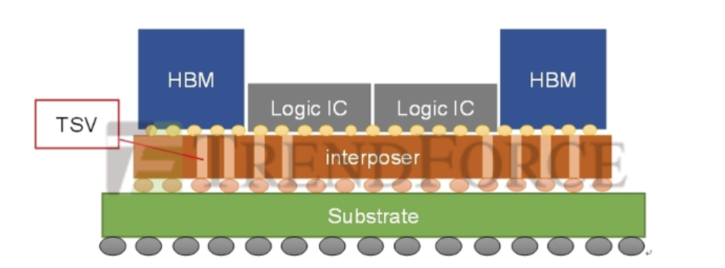 AI training and inference require increasing compute performance and memory bandwidth. Instead of placing every function on one large monolithic die, heterogeneous integration allows dies manufactured with different processes and serving different functions to operate together in one package.
As the number of compute dies and HBM stacks increases, the required interposer area, signal density, and power‑delivery capability also increase. This creates several challenges:
CoWoS scaling therefore reflects a broader transition in AI hardware—from a single chip to a multi‑die computing system inside the package.
TSMC's CoWoS platform consists primarily of three architectures.
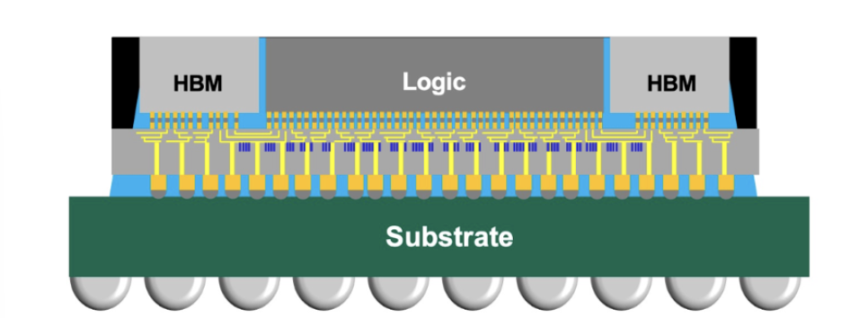
CoWoS‑S uses a silicon interposer to provide high‑density connections for high‑performance computing products. TSMC's official information states that CoWoS‑S currently supports silicon interposers of up to approximately 3.3 times reticle size, or about 2,700 mm².
A silicon interposer provides fine routing density. As the package grows, however, process complexity, cost, warpage, and interposer‑area limitations become more significant.
CoWoS‑R uses a redistribution‑layer interposer to connect SoCs and HBM. The RDL structure consists of polymer and copper routing and is relatively compliant. This helps support larger packages and provides mechanical buffering between the SoC and package substrate.
TSMC states that CoWoS‑R entered volume production in 2023.
CoWoS‑L combines an RDL interposer with local silicon interconnects. Silicon bridges are used only where dense die‑to‑die connectivity is required, while RDL extends the interconnect across the rest of the package.
 This architecture balances localised high‑density routing with large‑package scalability. TSMC recommends considering CoWoS‑L or CoWoS‑R when the required interposer area exceeds 3.3 times reticle size.
| Architecture | Primary interconnect | Engineering focus | | :--- | :--- | :--- | | CoWoS‑S | Large silicon interposer | High‑density routing, with greater scaling challenges at large sizes | | CoWoS‑R | RDL interposer | Package‑size flexibility and mechanical compliance | | CoWoS‑L | Local silicon interconnect plus RDL | Balance between local density and large‑package scaling |
The final choice depends on die arrangement, HBM count, signal density, thermal design, cost, and reliability—not package size alone.
In addition to scaling CoWoS horizontally, TSMC is continuing to develop its System on Integrated Chips, or SoIC, 3D‑stacking platform.
SoIC uses die‑to‑die or wafer‑to‑wafer integration to shorten vertical connections. According to TSMC's published roadmap, A14‑on‑A14 SoIC is scheduled for production in 2029, with 1.8 times the die‑to‑die I/O density of N2‑on‑N2 SoIC.
When SoIC and CoWoS are combined, the system can scale both vertically and horizontally. Package development is no longer simply a substrate selection task; dies, HBM, interconnects, power, cooling, and test must be considered together.
The source article also discusses CoPoS—Chip‑on‑Panel‑on‑Substrate—which extends wafer‑level processing from a circular wafer to a rectangular panel. The goal is to improve area utilisation and support larger packages.
Panel‑level processing is attractive from a manufacturing perspective, but it introduces additional challenges:
Publicly available TSMC information confirms the 5.5‑ and 14‑reticle‑size CoWoS roadmap. It does not provide enough information to verify the reported CoPoS panel dimensions, materials, or volume‑production schedule.
CoPoS should therefore be treated as an important panel‑level packaging direction to monitor—not as a finalised set of design rules based solely on reported dimensions.
Large AI packages must ultimately be assembled onto a system PCB. As package size, weight, power, and BGA scale increase, the PCB team should evaluate the following early:
These issues should not be addressed one at a time after the PCB has been completed. Package models, power conditions, BGA data, cooling structures, and the PCB stackup should be cross‑checked during the early layout stage.
The move from 5.5‑reticle‑size CoWoS toward 14 reticle sizes and beyond shows that advanced packages are carrying increasingly complete computing systems.
For PCB teams, the goal is not necessarily to enter semiconductor‑package manufacturing. It is to develop the ability to understand large‑package behaviour and the associated power, thermal, mechanical, and assembly constraints.
Future DFM will go beyond confirming whether a PCB can be fabricated. It will need to determine whether the package, PCB, and complete system can operate together reliably.
If your AI server, high‑performance computing, or optical‑communications project is currently in layout, eCloud can help organise PCB stackup requirements, manufacturing constraints, and DFM confirmation items so that package‑to‑board risks can be identified before prototyping.
