August 20, 2026
As AI, high-performance computing (HPC), and multi-die integration continue to drive interconnect density upward, glass substrates have become an important topic in advanced packaging. The market, however, is also filled with claims that can easily create confusion—for example, that glass will soon replace conventional PCBs, that certain AI processors have already moved entirely to glass, or that a specific year will mark the beginning of immediate mass adoption. For PCB manufacturers, the more useful questions are what glass substrates are designed to replace, which engineering problems they address, and how they may change customer requirements. The short answer is that glass substrates are not expected to directly replace conventional FR-4 multilayer PCBs in the near term. Their primary target is the organic core substrate and selected interposer functions inside advanced semiconductor packages. This is a different layer from server motherboards, control boards, and conventional HDI PCBs.
Advanced AI devices no longer rely only on scaling a single large die. They increasingly integrate logic dies, I/O dies, and high‑bandwidth memory (HBM) within one package.
As package size and interconnect count increase, organic package substrates must address several challenges simultaneously:
This does not mean that ABF and other organic materials are no longer usable. It means that some large, high‑density package designs are approaching the economic or technical boundaries of existing material and process platforms.
Intel states that glass offers improved flatness and thermal and mechanical stability, potentially supporting larger package sizes and higher interconnect density. Intel's original roadmap targeted complete glass‑substrate solutions for the latter half of the decade; it did not state that glass had already replaced organic substrates across the industry.
The value of glass is not that it is inherently a “more advanced” material. Its value lies in physical properties that can be tailored to package requirements.
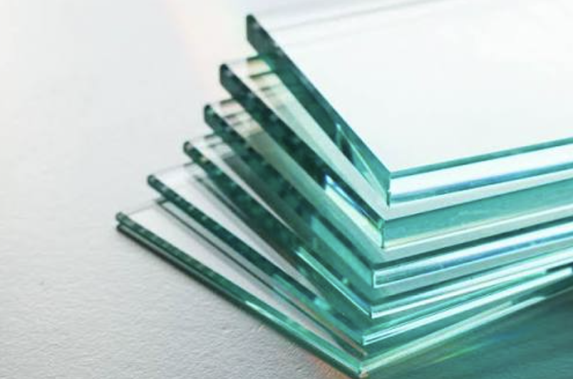
The coefficient of thermal expansion of glass can be adjusted through material composition. Glass can also provide strong flatness and dimensional stability. In large multi‑die packages, these characteristics can support finer registration and better warpage management.
However, saying that glass can reduce warpage is not the same as saying that glass eliminates warpage. Final performance still depends on glass thickness, copper distribution, the RDL stack, package materials, die placement, and assembly temperature profiles.
A through‑glass via (TGV) is a microvia formed through a glass core and then metallised or copper‑filled to carry power and signals vertically through the substrate.
Intel has published platform‑specific comparisons between conventional mechanical vias in organic cores and TGVs in glass‑core substrates, demonstrating the potential for higher via density. These figures reflect Intel's process conditions and should not be treated as universal specifications available from every supplier.
The electrical and optical characteristics of glass make it an interesting platform for research into high‑speed interconnects, embedded passive devices, and potentially optical interconnects.
Glass, however, is not the only possible platform for optical integration. Co‑packaged optics may also incorporate silicon photonics, polymer waveguides, organic substrates, or other packaging architectures. It would therefore be inaccurate to claim that only glass can support optical integration.
Because glass is brittle, production must address:
Samsung Electro‑Mechanics has publicly demonstrated a glass‑core package substrate and identified improved warpage and signal‑loss performance in large substrates as development goals. A technology demonstration, customer sampling, and stable volume production, however, are three different stages and should not be treated as equivalent.
Glass‑core substrates initially compete with selected materials and structures used in high‑end package substrates. AI server motherboards, power boards, networking boards, equipment controllers, and most industrial PCBs will continue to require FR‑4, high‑speed low‑loss laminates, and HDI processes.
A small or midsize PCB manufacturer therefore does not need to purchase TGV or glass‑processing equipment simply because glass substrates are receiving market attention.
The glass‑substrate supply chain requires laser processing, plating, cleaning, inspection, automated handling, and reliability‑testing equipment. These systems require their own control boards, power boards, high‑speed data‑acquisition boards, and test‑interface boards.
PCB manufacturers can begin by mapping customers in areas such as:
AGC has included glass‑core substrates for next‑generation semiconductor packaging in its published business plans, further indicating that material suppliers are continuing to build relevant capabilities.
Even when a PCB continues to use organic materials, it may operate in the same system as a large glass‑core package. Design teams will need to evaluate the following earlier in development:
DFM should therefore extend beyond trace width, spacing, and hole diameter. Package structure, stackup, materials, assembly conditions, and mechanical constraints must be reviewed together.
As of 2026, glass substrates are moving beyond a purely laboratory topic toward more concrete collaboration among material suppliers, equipment manufacturers, and advanced‑packaging companies.
For example, Intel and Lens Technology announced a collaboration in 2026 focused on exploring and accelerating glass‑based advanced‑packaging solutions. The announcement did not state that glass had already entered universal mass production across all AI processors.
For PCB manufacturers, the more practical next step is to map relevant customers, track package requirements, develop cross‑material DFM capabilities, and base equipment investments on actual sampling programmes, qualification requirements, and order visibility.
If your next AI, optical‑communications, or high‑speed computing project is currently in layout, eCloud can help organise PCB manufacturing constraints and DFM confirmation items so that risks across the package, materials, and system board can be identified earlier.
