From Sheet Resistance to Artwork and Test Data
Connect every embedded resistor to its material, copper terminals, fabrication geometry and acceptance requirements.
The board surface is crowded, but termination resistors still need to remain close to critical signals. Moving a resistor may add routing or vias. Embedded resistors can become an option worth evaluating.
The transition from schematic to fabrication introduces an easily underestimated question: once the resistor is inside the board, which documents tell the fabricator where copper remains, where resistance is formed and what value must be measured?
An embedded resistor PCB release must define geometry, materials, electrical connections and acceptance requirements together.

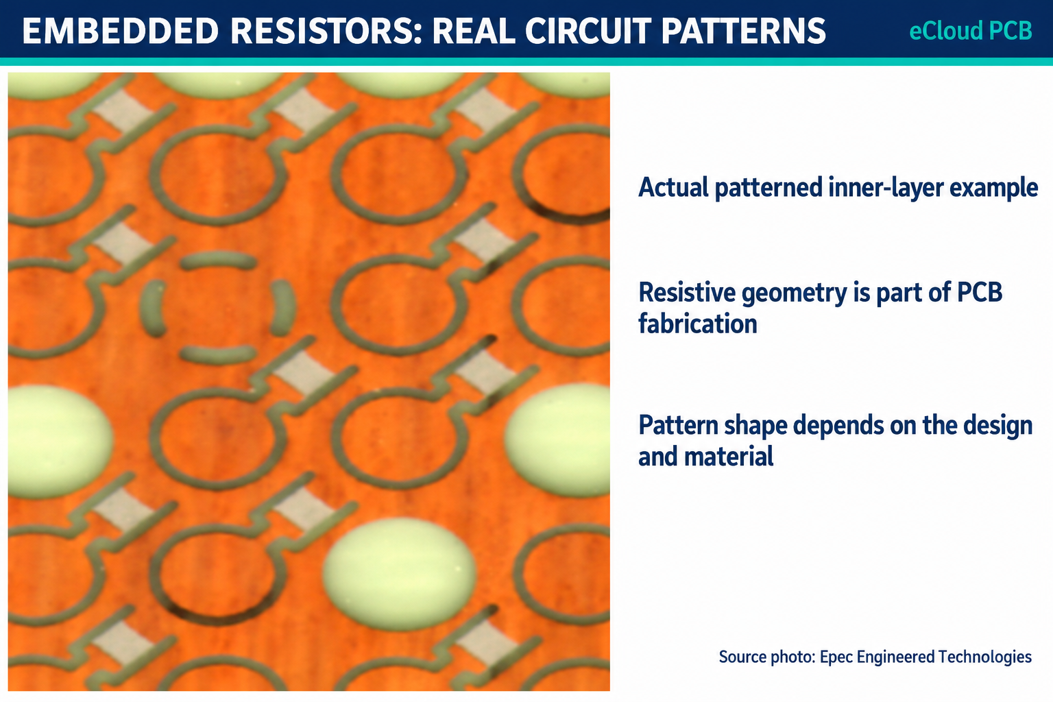
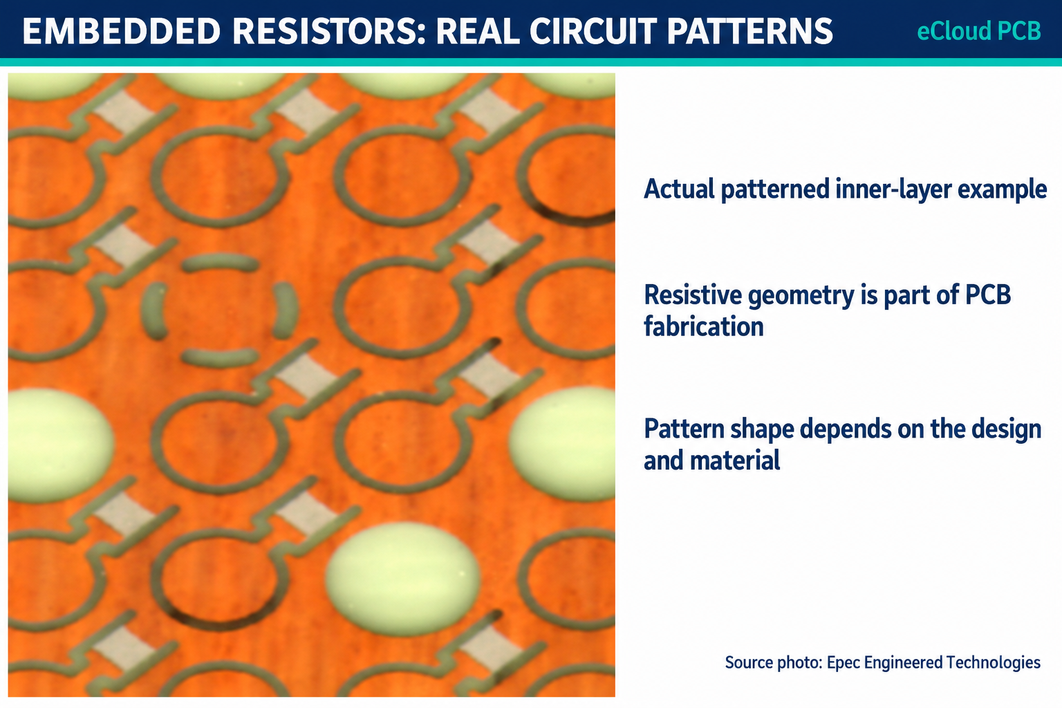 Embedded resistance integrates resistor functions into the PCB structure. Implementations include thin-film and thick-film technologies. This article focuses on resistive copper foil that is patterned to form planar thin-film resistors.
These materials combine copper with a resistive film. Processing retains copper terminals and conductors while removing copper above designated regions, allowing current to pass through the resistive film. Subsequent lamination encloses the structure.
For example, OhmegaPly uses a nickel-phosphorus (NiP) resistive alloy, while the TCR family includes nickel-chromium (NiCr) and other material options. Equal sheet resistance alone does not establish interchangeability.
Embedding can remove some surface components and their solder joints and may shorten interconnections. However, the finished resistance is established by PCB materials and processing, and replacement becomes less accessible. Circuits requiring repeated value changes should first consider the flexibility of surface-mounted resistors.
 References: OhmegaPly material construction, TCR thin-film resistive materials
 Sheet resistance, Rs, is expressed in Ω/□ and describes the electrical resistance characteristic of a uniform film. For a simple, uniform rectangular resistor, nominal resistance can be estimated as:
R = Rs × L/W
Where:
For an illustrative geometry using 25 Ω/□ material, L = 0.50 mm and W = 0.25 mm:
25 × 0.50/0.25 = 50 Ω.
This does not mean that 25 Ω/□ material can only produce 25 Ω resistors. Nor do different-sized resistors with equal resistance necessarily have equal power capability.
Finished values remain affected by material uniformity, etching and subsequent processing. Serpentine and other complex patterns also require more than unmodified application of the straight-bar formula.
The 50 Ω resistor value discussed here is a different specification from the 50 Ω characteristic impedance of a transmission line.
References: Sheet resistance, geometry and power considerations, Processing effects on finished resistance
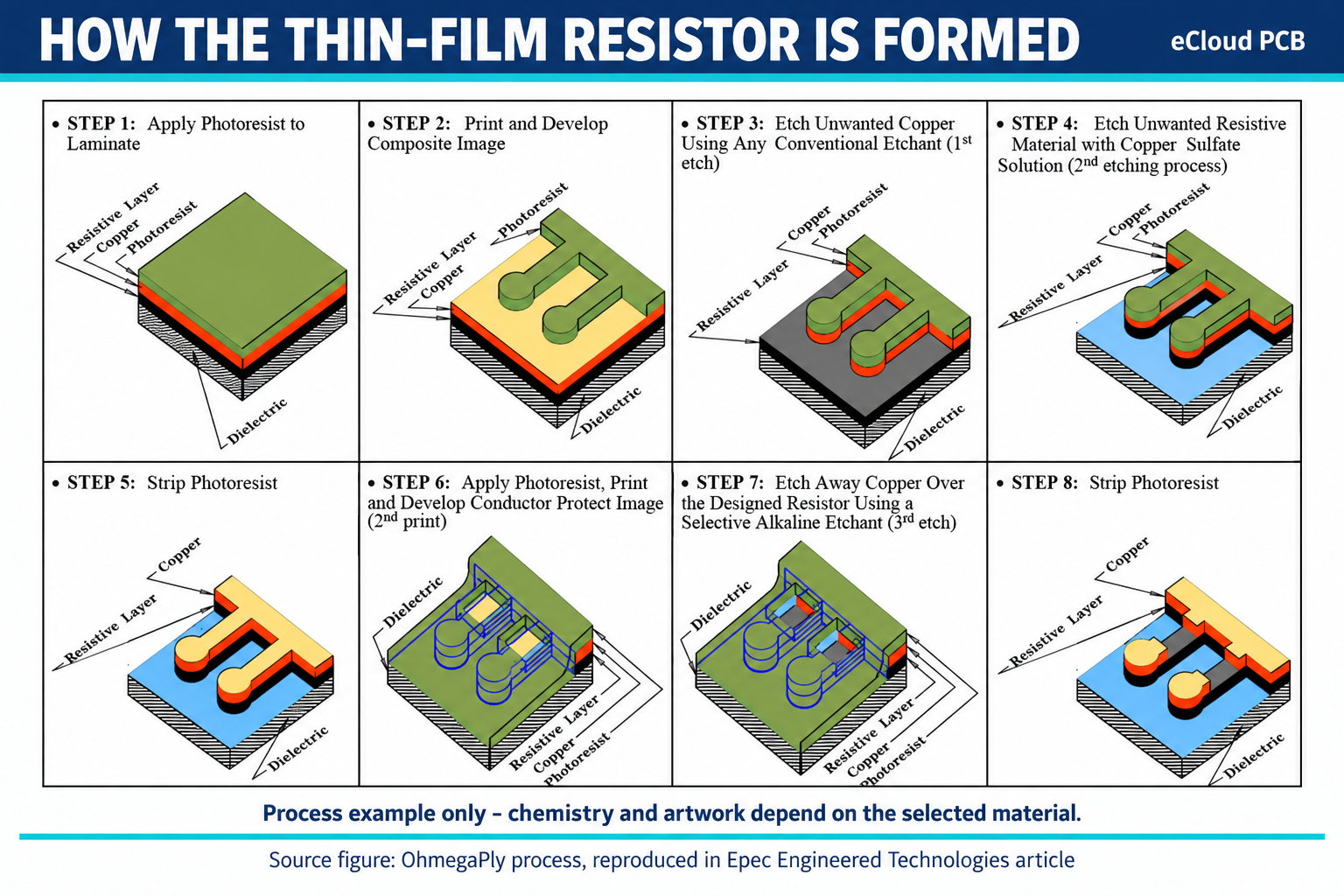 One physical circuit layer containing thin-film resistors may require multiple process images. It cannot simply be released as an ordinary internal copper layer.
The fabricator must be able to identify at least:
For example, the OhmegaPly subtractive process includes patterning the overall geometry and separately defining resistor length. Final copper geometry, active resistor geometry and process copper-removal images are therefore not interchangeable.
The designer should define the final intent. Selective-etch extensions, registration allowances and compensation must be confirmed for the material and fabrication process.
A resistor-definition data layer does not necessarily represent an additional physical copper layer.
Reference: Thin-film resistor design and process-image guide
The following checklist and filenames are examples, not universal production-phototool specifications. Confirm the receiving fabricator’s data requirements before exporting.
Provide the full copper, solder mask, outline and NC Drill data, together with ordinary fabrication requirements. Use Gerber, ODB++ or another agreed format accepted by the fabricator.
Resistor-specific data does not replace the complete PCB fabrication package.
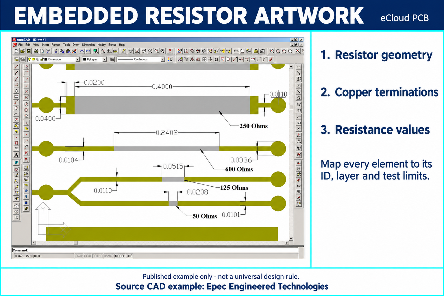 For resistors located on L3, the following names can express the logical design intent:
L03_Cu_Intent.gbr: final retained-copper intent, consistent with the complete PCB data.L03_ER_Body.gbr: active resistor-region geometry.L03_ER_Map.pdf: an overlay identifying resistors, dimensions and necessary location information.If the fabricator requests first- and second-exposure images directly, export according to its definitions. Renaming the logical layers above does not turn them into valid process images.
Keep resistor geometry separate from identification and dimension annotations to prevent text or dimension lines from being interpreted as fabrication features.
Provide documents such as Layer_Map.pdf and Stackup.pdf defining:
“Embedded resistor on L3” or “positive image” alone does not fully establish the image’s manufacturing purpose.
Provide an ER_Schedule.csv or spreadsheet containing at least:
“BR1, 50 Ω, ±10%, 45–55 Ω” is only an example of acceptance fields. It does not establish a fabrication commitment to that tolerance.
Supply a netlist containing embedded-resistor information or a resistor mapping file that can be merged with it. Define test nodes, expected values and limits.
Also establish how testing will be performed at the inner-layer and finished-board stages, and whether the measurement current and voltage are appropriate. With series or parallel paths, determine whether the measurement represents an individual resistor or an equivalent network.
Retain embedded-resistor identifiers and values in the circuit and fabrication documentation. Clearly identify them in the assembly release as “formed during PCB fabrication; no component procurement or placement required.”
Where surface resistors remain in the circuit, distinguish them clearly to prevent duplicate procurement or assembly omissions.
If resistor geometry is stored on a dedicated mechanical layer, verify that the layer is actually selected for export. The ability to export a mechanical layer does not mean the tool automatically understands its resistor function or checks every electrical relationship.
Reload the exported files into a CAM viewer and confirm:
Even with ODB++, confirm that the fabricator receives and interprets the custom resistor data correctly. The format name alone does not establish completeness.
References: Fabrication-output configuration, Mechanical layers in manufacturing outputs
An ordinary bare-board test that does not recognize embedded resistors may interpret an intentional resistance as an abnormal high-resistance connection. Passing continuity testing alone also does not establish compliance with the required resistor value.
Test data must therefore include resistor locations, expected values and acceptance limits, with appropriate measurement conditions. AOI can inspect geometry but cannot replace resistance measurement.
Precision tolerances or trimming requirements also need advance confirmation of the process, accessible processing stage and validation method. Do not assume that resistor values can be freely adjusted after lamination.
Reference: Electrical testing of embedded passive components
A releasable embedded resistor PCB package connects sheet resistance, resistor geometry, copper terminals, physical layers and acceptance requirements. These definitions give the fabricator a basis for process evaluation and the R&D team a basis for accepting the finished board.
If your project is considering embedded resistors, provide eCloud with target resistance, tolerance, operating conditions, stackup and preliminary geometry to discuss material and process feasibility. Actual acceptance scope and export requirements should be confirmed before production.