Mask-Opening and Assembly Trade-offs for Fine-Pitch Pads
Calculate the remaining dam before retaining it, reducing expansion or choosing a gang opening.
The Gerber files have been released, but the fabricator returns an engineering question: “The solder mask dam is too narrow here. Please approve a gang opening.”
For an R&D engineer, neither answer is automatic. Retaining the dam may create fabrication concerns, while removing it raises questions about solder bridging during SMT assembly.
First establish the remaining dam width, whether it can be fabricated consistently, and what the assembly process must accommodate after the opening changes.
Solder mask dam design requires coordinated review of three geometries: copper, solder mask and solder paste.
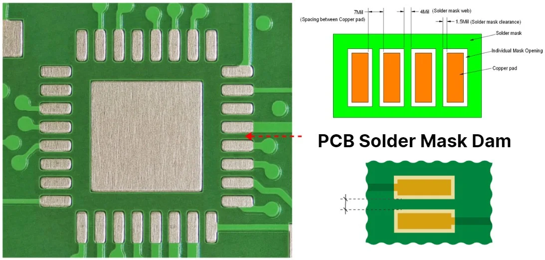 A solder mask dam, also called a web, is the solder mask material retained between adjacent mask openings.
It helps limit solder wetting in non-soldering areas and reduces the risk of bridging between adjacent joints.
A solder bridge is an unintended solder connection between joints that should remain separate.
However, a mask dam does not guarantee freedom from shorts. Paste volume, stencil apertures, component displacement and reflow conditions also affect the final joints.
Consequently, a bridging investigation should extend beyond mask dams, and a design without individual dams should not automatically be classified as defective.
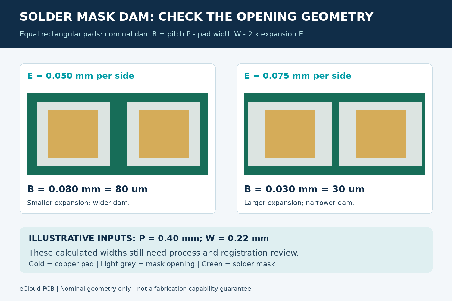 Solder mask dam width is not the same as the copper edge-to-edge spacing.
For two equal-width rectangular pads arranged side by side, define the following along the pitch direction:
Then:
B = P − W − 2E
For an illustrative pitch of 0.40 mm and pad width of 0.22 mm, the copper gap is 0.18 mm.
With 0.05 mm expansion per side, the nominal dam is:
0.40 − 0.22 − 2 × 0.05 = 0.08 mm, or 80 μm.
Increasing expansion to 0.075 mm per side leaves:
0.40 − 0.22 − 2 × 0.075 = 0.03 mm, or 30 μm.
The copper pads have not changed, yet the nominal dam has fallen from 80 μm to 30 μm. This illustrates why a board-wide default expansion may be unsuitable for fine-pitch components.
These are geometric examples, not package recommendations or guarantees of finished dam width. For unequal, circular or irregular openings, inspect the actual minimum distance between opening boundaries.
Some component application guides recommend a mask web of approximately 75 μm. That does not establish the same capability for every ink, color, copper thickness or exposure process.
The fabricator must also evaluate imaging and development capability, copper topography, ink conditions and mask registration.
Two questions need separate answers:
Adequate nominal dam width does not establish adequate registration margin. Conversely, enlarging an opening to provide registration margin may remove the available dam.
When ordering, establish whether a quoted limit is a design value, a fabrication-compensation value or a finished-board acceptance requirement.
References: QFN/SON mask openings and fabrication capability, Examples of rules for different mask processes
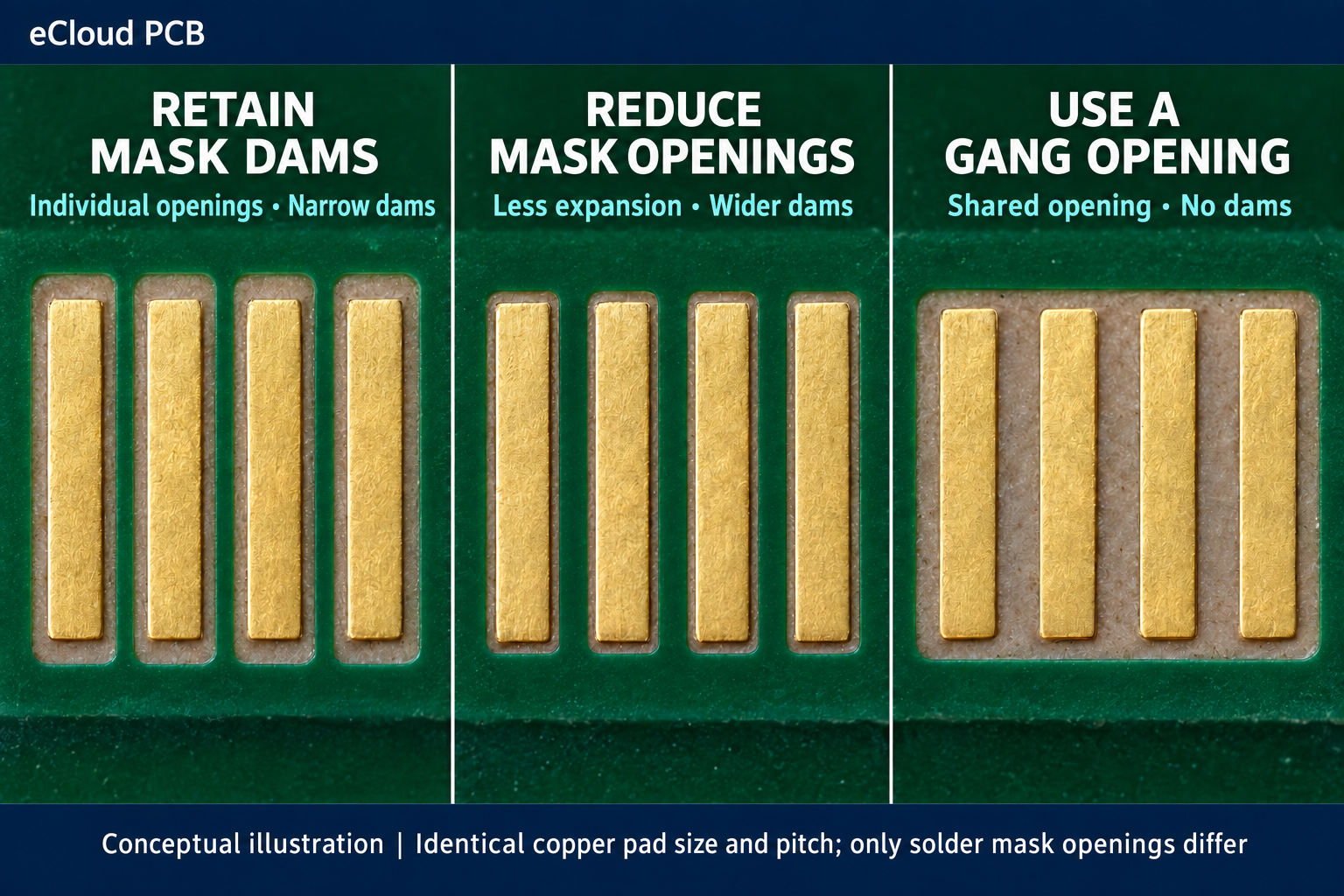
If the actual construction fits the fabricator’s stable processing capability, individual openings can be retained.
Confirm the finished dam, registration and pad-exposure conditions rather than relying on a thin line visible in CAM.
Reducing expansion increases nominal dam width, but registration margin and the available soldering area must be reviewed at the same time.
For a non-solder-mask-defined (NSMD) design, do not reduce the opening over the copper edge merely to retain a dam without evaluating the resulting change to a solder-mask-defined (SMD) land.
SMD lands are not universally unsuitable. Their use should follow the actual component’s package guidance and assembly requirements.
Some fine-pitch package guides allow or recommend a shared opening, such as a trench along a row of pads.
Analog Devices’ LFCSP guide includes a trench-opening example for fine-pitch conditions, demonstrating that the absence of individual mask dams can be an evaluated design choice.
Before making that change, check whether the opening will expose traces, copper areas or vias that were intended to remain covered, and obtain assembly review.
Reference: Individual and trench-opening examples for fine-pitch LFCSPs
Keep these three data layers distinct:
Changing the mask to a gang opening does not mean the stencil should have one continuous slot. Adjacent copper pads remain separate, and paste printing should be designed for the individual joints and assembly process.
Without mask separation between pads, the assembler needs to confirm stencil, paste-printing and placement conditions, with first-article inspection where appropriate.
A mask dam does not replace assembly validation, and fabrication feasibility does not by itself establish good SMT solderability.
Reference: Coordinating land patterns, mask and stencil design
Ask the fabricator to identify the component location, original openings and proposed modification area. Then review:
Include the approved opening strategy in the production data. Changes affecting pad definition or exposed copper should be confirmed before fabrication.
Solder mask dam design balances dam width, registration margin, pad definition and paste printing. Smaller openings, individual dams and gang openings should each have a clear fabrication and assembly basis.
For a fine-pitch PCB prototype, provide eCloud with the Gerber files, component part numbers and critical mask requirements to discuss DFM review items and resolve opening changes before production.