M8/M9 High-Speed PCB Series | Part 2
Understand tool wear, smear and hole preparation, then define the interconnect validation requirements.
Once a high-speed PCB material has been selected, R&D attention often shifts to impedance and trace-width compensation. In a multilayer board, however, stable connections between internal layers and plated through-holes also depend on the condition left by drilling.
A hole that meets its diameter requirement is not necessarily ready for plating. Passing the shipment electrical test also does not replace interconnect verification after thermal stress.
M8/M9 high-speed PCB drilling should therefore be reviewed as a connected sequence of material behavior, cutting, hole preparation and reliability.
Mechanical drilling cuts through copper, resin and glass in succession. These materials respond differently to cutting, while the tool must also evacuate debris from the hole.
Greater board thickness, smaller holes, heavier internal copper or a different glass construction can change chip evacuation and cutting loads. Even within one material series, a different board construction may require different processing parameters.
The statement that “M8/M9 is always harder to drill than every FR-4 material” is therefore too broad. Review the exact material, drill diameter, drilling thickness and copper distribution before defining the process.
For example, a low-loss material processing guide may call for adjustments to cutting speed, feed per revolution and drill-stack conditions relative to standard FR-4. Those recommendations remain specific to that material.
Reference: Low-loss material drilling and hole-preparation guide
 Drill wear describes a change in tool condition. A dull cutting edge can change cutting and friction behavior, potentially affecting diameter, burrs, hole walls and positional stability. Appearance alone does not establish that wear caused every defect.
Glass-fiber protrusion or pull-out describes locally uneven material removal. Fibers may remain incompletely cut and extend into the hole, or be pulled out and leave cavities. These conditions require investigation of cutting, support and material construction; they should not automatically be classified as resin smear.
Resin smear refers to resin residue or coating produced during drilling. Of particular concern is whether it covers the exposed inner-layer copper connection surface. Copper deformation and loose debris should also be identified separately rather than grouped under “smear.”
Defect identification should combine drilled-hole inspection with subsequent microsections and, where necessary, suitable microscopic analysis. A schematic can explain a mechanism but cannot establish an actual defect condition.
Spindle speed, feed rate and feed per revolution are related. Dividing feed rate in mm/min by spindle speed in rev/min gives feed per revolution in mm/rev.
Reducing feed rate without considering spindle speed and tool conditions does not necessarily improve the hole wall. Increasing spindle speed alone does not guarantee better cutting quality either.
Using the material guide and trial-drilling results, the fabricator should evaluate:
Tool hit count is one control variable. A number shown in an illustration should not become a universal requirement for every M8/M9 construction.
Desmear removes resin residue that can obstruct internal-layer interconnection and supports subsequent hole-wall metallization. Insufficient treatment can leave contamination; excessive treatment can produce unnecessary resin recession or interface damage.
Chemical desmear, plasma treatment or a combination should be selected for the actual resin system, board thickness, hole diameter and production line. Low-loss materials do not universally require additional plasma, and a longer chemical exposure does not necessarily produce a better result.
Desmear also serves a different purpose from deliberate resin etchback. For example, the original processing guide for certain high-frequency materials explicitly advises against etchback, illustrating why processes cannot be transferred unchanged between materials.
Reference: High-frequency material drilling and hole-preparation requirements
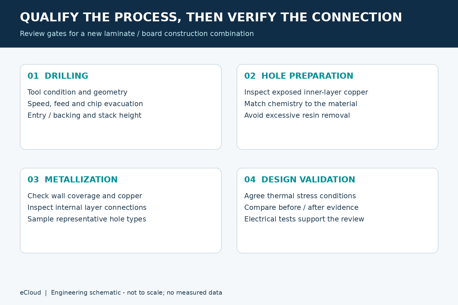 Prototype validation should first establish which stage can reveal the issue being investigated.
Inspection after drilling can reveal burrs, debris and wall morphology. After desmear, attention should shift to exposed internal copper and resin removal. Following metallization and plating, coverage, hole copper and internal-layer connections can be examined.
For projects with high reliability requirements, agree on applicable thermal-stress or thermal-cycling conditions and assess interconnect condition before and after exposure. Room-temperature continuity, impedance testing and microsections answer different questions and cannot replace one another.
Sampling should cover representative constructions, including the smallest holes, higher aspect ratios and different hole types, rather than only convenient locations. Test items, quantities and acceptance criteria should be agreed in advance for the product.
Moisture control and baking should also be defined by material and process stage. Prepreg, cores, laminated subassemblies and finished boards have different handling requirements; a single temperature and duration should not be applied to all of them.
The priority in M8/M9 high-speed PCB drilling is to establish the processing conditions required by the material and board construction, then connect drilling, desmear, plating and verification.
Stable interconnect structures are needed to support the electrical benefits of low-loss materials. For a prototype review, provide eCloud with the material part number, board thickness, minimum hole diameter, hole structures and validation requirements to discuss fabrication conditions and items requiring advance confirmation.