From Advanced Packaging to System Co-Design
Explore the TPCA forum’s integration message through escape routing, stackup planning, and power delivery.
The chip has been selected, a reference design is available, and the project appears ready to move forward.
Then layout begins. The BGA escape routing requires a different via approach. A stackup revision changes the impedance conditions. Power delivery and decoupling components compete for limited space, while the manufacturer identifies additional constraints.
Each issue may be manageable, yet changing one area can affect several others.
This is why PCB heterogeneous integration matters to hardware R&D teams. As more functions are integrated within a package, board designers still need to address its connections to power delivery, signals, cooling, and manufacturing.
On October 23, 2025, TPCA Show hosted the Semiconductor and PCB Heterogeneous Integration Summit. Moderated by Zhen Ding President Chien Chen-Fu, the forum brought together Shih Chin-Tay, ASE’s Hung Chih-Pin, and Zhen Ding Chairman Charles Shen to discuss links between semiconductors, advanced packaging, and PCBs.
According to Central News Agency’s on-site report, Hung positioned PCBs as a critical part of integration platforms and discussed developments including packaging and silicon photonics. Shih emphasized cooperation and strategic alliances.
In Zhen Ding’s post-event statement, Shen described the PCB’s expanding role from signal connectivity to system support, with power distribution, signals, and thermal performance considered together.
Our interpretation for R&D workflows is that constraints across these disciplines need to be coordinated earlier, allowing specialists to define a feasible design together.
Statements about the boundaries between semiconductors and PCBs becoming blurred can suggest that system boards must adopt the manufacturing dimensions used inside chips or packages.
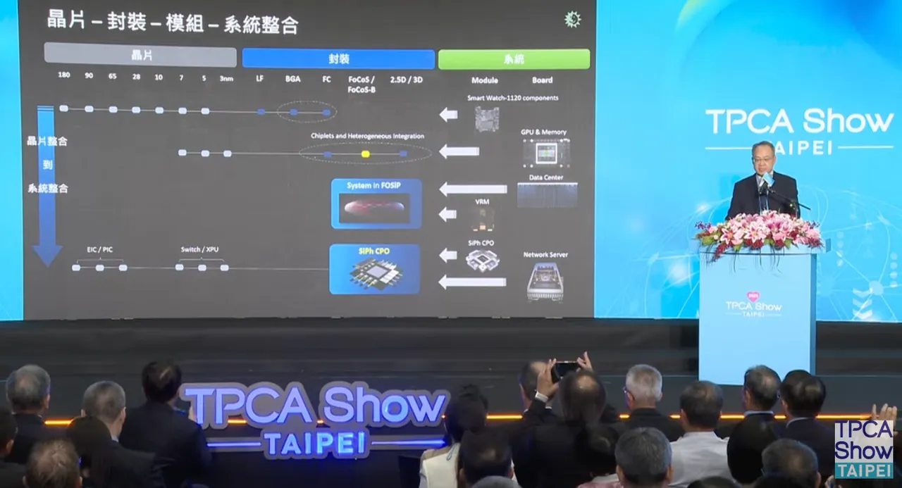
Chips, internal package interconnects, package substrates, and system PCBs still serve different functions and operate under different manufacturing conditions. Advanced packaging can integrate multiple chips through interposers, redistribution layers, or die stacking. These structures should not be equated with motherboard traces and vias.
GUC’s advanced packaging overview likewise distinguishes internal packaging interconnects from chip-package-PCB co-design.
For board-level engineers, the starting point is the selected package’s pinout, escape-routing requirements, and electrical guidance. These inputs help determine whether HDI is needed, which via structures are appropriate, and how much routing capacity is required.
Industry trends establish direction. The actual package requirements establish the starting point for the board.
Consider a hypothetical project in which the main component placement is complete before the team discovers that the densest BGA cannot be escaped using the planned via structure.
Changing the vias may affect routing-layer assignments, dielectric thicknesses, and manufacturing processes. The trace widths originally reserved for controlled impedance may also require recalculation.
Although hypothetical, this example illustrates a practical relationship: stackup, escape routing, and manufacturing conditions influence one another.
Intel’s PCB stackup guidance identifies BGA escape requirements, power planes, and component density as important stackup-planning factors.
Before extensive routing begins, teams should:
If a manufacturing proposal changes the specified material, dielectric thickness, or via structure, obtain design approval and update the controlled revision to preserve a clear fabrication baseline.
A power supply’s or regulator’s rated output is the starting point for power-delivery assessment.
When load current changes, PCB power distribution impedance and decoupling arrangements also affect voltage at the device. Texas Instruments’ power-layout guidance explains how routing parasitics and decoupling connections influence transient power delivery.
The engineering implication is that power requirements and physical layout should be reviewed together.
Is sufficient space available for appropriate decoupling placement? Do power and ground connections create unnecessarily long paths? Has dense escape routing displaced resources originally reserved for power delivery?
These questions are best addressed while placement and stackup can still be adjusted. Investigating them after a prototype exhibits instability can add troubleshooting and revision work.
The cooperation and strategic alliances discussed by Shih need concrete information and clear responsibilities at the project level.
R&D, layout, materials, fabrication, and assembly teams can jointly confirm:
This checklist is our practical recommendation based on the forum’s integration theme; it is not a verbatim conclusion from the speakers.
As cooperation becomes more extensive, revision control, change records, and verification criteria become more important. Otherwise, each team may complete its work according to a different interpretation, with the mismatch appearing only during integration.
PCB heterogeneous integration encourages R&D teams to address interdependent decisions earlier.
Evaluate escape routing when selecting the package. Confirm power delivery and manufacturing conditions when planning the stackup. Define verification activities when arranging prototypes.
This gives later changes a clearer basis and makes prototyping a more purposeful engineering exercise.
If your next project involves dense escape routing, material substitution, or controlled-impedance stackup changes, share the Gerber files, stackup, and fabrication requirements with eCloud before PCB prototyping. Together, we can identify the engineering conditions that need clarification before fabrication proceeds.