TPCA Special 02 | Connecting Design Decisions with Manufacturing
Align materials, stackups, and validation requirements before committing the design to fabrication.
The chip has been selected. Interface requirements are confirmed. Layout is almost complete.
Then the PCB fabricator replies: the specified thickness is unavailable, the stackup needs adjustment, and trace widths must be recalculated.
The project manager asks, “Can we still keep the delivery date?”
For hardware R&D engineers, the pressure of AI hardware development appears in exchanges like these. High-speed PCB design extends from circuits and routing to material availability, fabrication conditions, and the question of what the finished prototype must actually demonstrate.
The 2026 TPCA leadership forums bring high-speed transmission, advanced materials, system collaboration, and global manufacturing into the same discussion. For development teams, that raises a practical question: As specifications advance, how do we establish a design that can be fabricated, validated, and reproduced?

This year’s TPCA Show × CommonWealth leadership summit focuses on supply-chain upgrades driven by AI computing demand. The AI empowerment and global deployment forum addresses the transition from technical breakthroughs to global production and supply-chain resilience.
Both themes offer the same reminder for R&D: chip requirements, PCB construction, and manufacturing conditions need to be aligned during development.
For example, reliable operation of a high-speed interface requires consideration of the complete channel formed by the chip package, traces, vias, and connectors. Material selection is one decision within that process.
AI servers, edge-computing products, and endpoint devices also differ in board dimensions, channel lengths, power consumption, and cost constraints. Adding AI functionality does not automatically justify applying the same advanced PCB specification to every product.
The first step is to document the requirements: Which channels are critical? What loss is acceptable? Which conditions require system-level testing?
References: TPCA leadership summit topics and AI empowerment and global deployment forum topics.
“Does this board need a lower-loss material?”
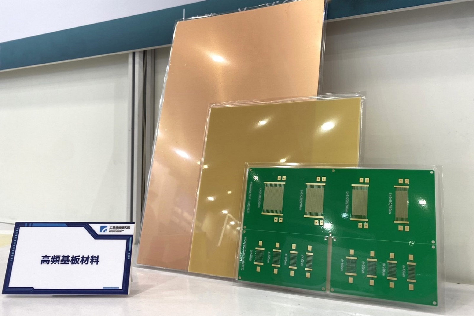
Before answering, establish the interface requirements, channel length, and available loss budget.
Dk, or dielectric constant, and Df, or dissipation factor, are important material properties. Actual channel performance also depends on copper roughness, trace geometry, and dielectric thickness. Material comparisons must account for the frequency and test conditions associated with the published data.
A material upgrade should therefore address an identified design issue. Lower-loss material deserves consideration when the loss of a longer route approaches its limit. If vias or connectors are the main constraint, those structures also need attention.
Identify where channel margin is being consumed before deciding how to change the material and construction. This gives any additional cost a clear engineering basis.
Reference: Altera PCB stackup selection guideline.
Consider a hypothetical situation: a team completes most routing using a reference design, then learns that the specified core and prepreg combination cannot be supplied as planned.
 Changing dielectric thickness requires a new review of impedance trace widths and spacing, including whether the existing routing has enough room. One material decision can affect completed layout work.
Before routing critical channels, obtain a manufacturable stackup from the fabricator. Confirm the materials, dielectric thicknesses, copper thicknesses, and impedance geometry. Design for manufacturability, or DFM, should be part of this stage.
If backdrilling is needed, confirm the processing layers, residual stub requirements, and fabricator capability early. Whether to use it should follow channel analysis. Via stubs affect high-speed signals, so their treatment should be resolved before shipment.
References: High-speed stackup design and manufacturing considerations and TI high-speed interface layout guidelines.
When forums discuss global manufacturing, development teams need to ask a further question: If the production site or supplier changes, which conditions must remain consistent, and which changes require validation?
One study of high-speed serial links rebuilt an existing design with another fabricator and measured a substantial reduction in via bandwidth. The case shows why manufacturing details deserve a place in design documentation. It does not establish that every supplier transfer will produce the same result.
If the documentation contains only Gerber files, overall board thickness, and a material family name, conditions may still need to be clarified during a transfer.
Retain the approved production stackup, material construction, impedance geometry, backdrilling requirements, and measurement methods. Establish a review process for material substitutions and engineering changes.
Impedance testing and full channel validation should also have separately defined purposes. Passing impedance results still leave insertion loss, reflections, crosstalk, or system operation to be assessed according to product requirements. During prototype acceptance, the team should understand which question each report answers.
Reference: Research on high-speed via design and fabrication transfer.
R&D engineers and project managers can start with five shared points of confirmation:
Earlier agreement makes the impact of later changes easier to assess and helps connect engineering confirmation with delivery planning.
The technical upgrades and supply-chain collaboration discussed at TPCA suggest a practical direction for development teams: bring more manufacturing conditions into early design decisions.
R&D needs to understand why a revision is feasible, what defines its production baseline, and which items require another review when conditions change.
When the team can answer those questions together, high-speed PCB design becomes easier to move from repeated email exchanges to an evidence-based release.
If your project is evaluating high-speed materials, an impedance-controlled stackup, or prototype fabrication conditions, share the existing stackup, Gerber files, and critical specifications with eCloud to clarify the engineering items that need confirmation before fabrication.