March 20, 2026
With the rapid advancement of high-speed digital communications, high-performance computing (HPC), and artificial intelligence (AI) hardware, the market now places unprecedented demands on printed circuit boards (PCBs) in terms of trace density, signal integrity (SI), and long-term reliability. High-layer-count PCBs, particularly those incorporating advanced High-Density Interconnect (HDI) and Any-layer HDI technologies, have become the core platforms supporting these cutting-edge applications. This article will provide an in-depth analysis of the manufacturing details behind these two cutting-edge technologies and explore the reliability challenges they face. We will also discuss why selecting a supplier with top-tier technical capabilities early in the project is critical to its success.
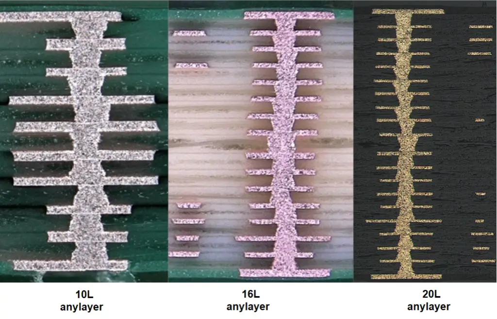
To understand these technologies, we must first look at their physical structures:
There are three main technological driving forces promoting the adoption of these advanced processes:
The production of any-layer interconnect is an extremely precise process with many variables. For quick understanding, we have summarized the core process steps, challenges faced, and industry countermeasures in the table below:
| Process Step | Challenges Faced | Countermeasures | | :--- | :--- | :--- | | Material Selection | Multiple laminations demand high dimensional stability and heat resistance (Tg, Td) from the substrate. High-speed applications need low-loss (Low Dk/Df) materials, but their adhesion to copper foil and processability differ from standard FR-4. | Scientifically select core materials, prepreg (PP), and copper foil based on signal rate and loss budget. eCloud leverages a vast material database to precisely balance performance, yield, and cost. | | Stack-up Design & Impedance Control | In boards with dozens of layers, trace widths and dielectric thicknesses on each layer must be precisely calculated (e.g., single-ended 50Ω, differential 100Ω). Any-layer interconnects can easily cause discontinuities in the return path, leading to signal issues like reflections or ringing. | Implement advanced electromagnetic field simulation software to optimize impedance, crosstalk, and insertion loss during the design phase, ensuring the integrity of adjacent reference planes. | | Laser Drilling & Via Metallization | Requires precisely drilling microvias (e.g., 50μm diameter) on dielectric layers thinner than 40μm. Subsequent plated via filling, if containing voids or unevenness, plants serious hidden hazards. | Invest in high-precision UV laser drills and optimize parameters; adopt advanced pulse plating formulas to ensure dense via filling. eCloud maintains extremely strict inspection standards in this area. | | Multiple Laminations & Alignment | Multiple lamination cycles easily lead to accumulated tolerances, causing blind via misalignment or opens. Repeated heating can also induce material deformation or delamination. | Implement high-precision LDI (Laser Direct Imaging) alignment systems, use substrates with high dimensional stability, and monitor lamination parameters via MES systems to keep errors within micron levels. | | Surface Finish & Fine Lines | Outer layer traces are extremely fine (line width/space reaching 30/30μm) and require surface finishes suitable for high-speed signals (e.g., ENIG, Immersion Silver). | Combine ultra-thin dry film or electroplated photoresist, and select surface finish processes that minimally impact insertion loss for high-speed applications. |
Fabrication is one thing; long-term stable operation is another. The reliability risks of high-layer-count any-layer HDI boards mainly focus on physical structural fatigue and electrical performance degradation:
Thermo-mechanical Reliability: Different materials (copper, resin, glass fiber cloth) inherently have mismatched Coefficients of Thermal Expansion (CTE). During severe temperature cycling tests or long-term high-temperature operation, stress concentration points like microvia interfaces or copper pillars are highly prone to fatigue fracture. Countermeasure: Must select material combinations with better CTE matching, optimize the plated via fill structure to enhance copper pillar fatigue resistance, and implement TCT (Temperature Cycling Test) and TST (Thermal Shock Test).
CAF (Conductive Anodic Filament) Risk: Due to the extremely thin interlayer dielectrics, under the combined assault of "high humidity" and "voltage bias," metal ions can easily migrate along glass fiber bundles or resin interfaces, forming CAF. This ultimately leads to decreased insulation resistance or even micro-shorts. Countermeasure: Strongly recommend using low-profile copper foil dedicated prepregs (PP) with spread glass or flat glass cloth design, strictly control hole wall quality, and implement rigorous CAF reliability validation.
Long-Term Signal Integrity (SI) Degradation: Environmental stress (e.g., prolonged temperature and humidity changes) can cause minor drifts in the properties of dielectric materials, subsequently affecting the accuracy of impedance control and leading to gradual signal integrity degradation. Countermeasure: Select high-frequency, high-speed substrates with low moisture absorption and stable characteristics from the source. Reserve sufficient performance margin during the initial hardware design phase to ensure smooth operation throughout the product's entire lifecycle.
In summary, advanced HDI and any-layer interconnect technologies are key to the bottlenecks of modern electronic hardware. However, the hidden process and reliability behind them should not be underestimated. During the project development phase, choosing a partner like eCloud, which possesses deep process expertise and can provide comprehensive support from material selection to electrical simulation, can significantly reduce trial-and-error costs and bring your innovative products to market faster.
