March 20, 2026
Welcome to the eCloud Technical Column! Today, we’ll take you on an in-depth exploration of an indispensable aspect of PCB design: silkscreen printing. Whether you’re a beginner just starting with PCB layout or a seasoned pro looking to refine your skills, mastering silkscreen design specifications not only makes your circuit boards look more professional but also significantly reduces error rates during the back-end assembly (PCBA) and repair processes. Below, we’ve compiled the basics of PCB silkscreen design along with 9 practical design tips!
Silkscreen refers to the text or graphics printed on the surface layer of a PCB. Its main purpose is to provide various practical information, helping engineers easily identify components during assembly and debugging. It can be letters, numbers, or text used to mark component values, reference designators, polarity, and even include board version and manufacturer information.
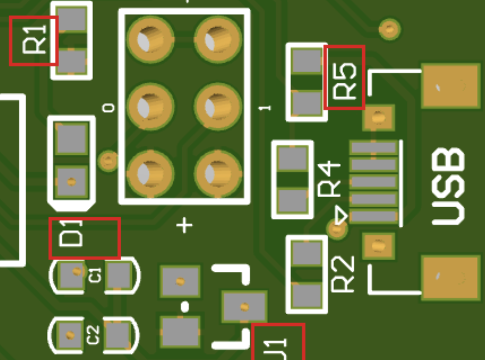
On a complete PCB, the silkscreen typically covers the following important information:
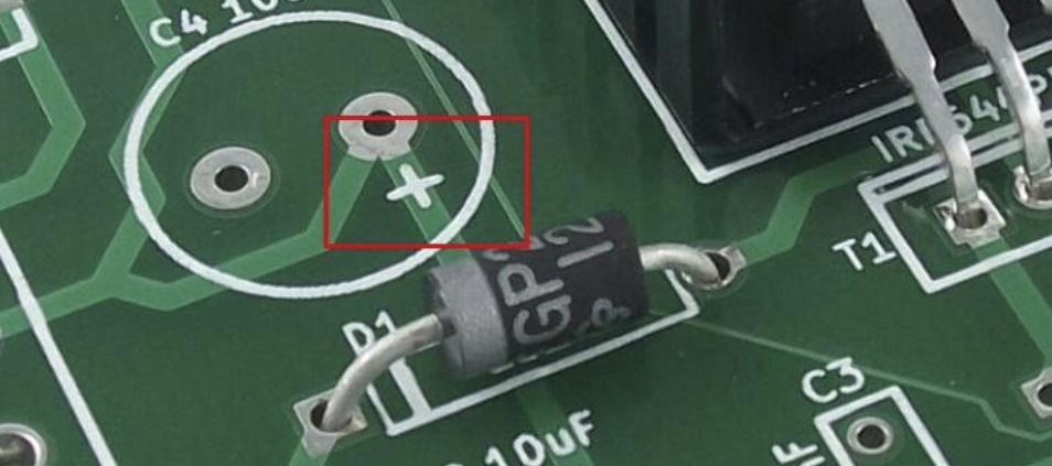
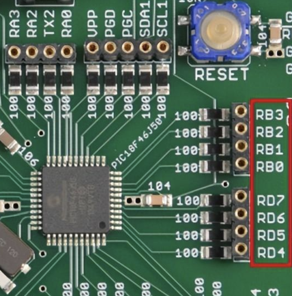

Generally, white is the most common silkscreen color because it provides the highest contrast with most solder mask colors (like the common green solder mask) and is the most manufacturing-friendly for PCB fabricators.
In the initial design phase, yellow, red, or black are sometimes used. As for pink... although some layout engineers think it looks cool, it's generally not recommended because its ink characteristics are less friendly to subsequent manufacturing processes!
In PCB design software, the silkscreen layer is typically defined on the Top Overlay or Bottom Overlay.
Currently, there are three main methods for creating silkscreen in PCB manufacturing:
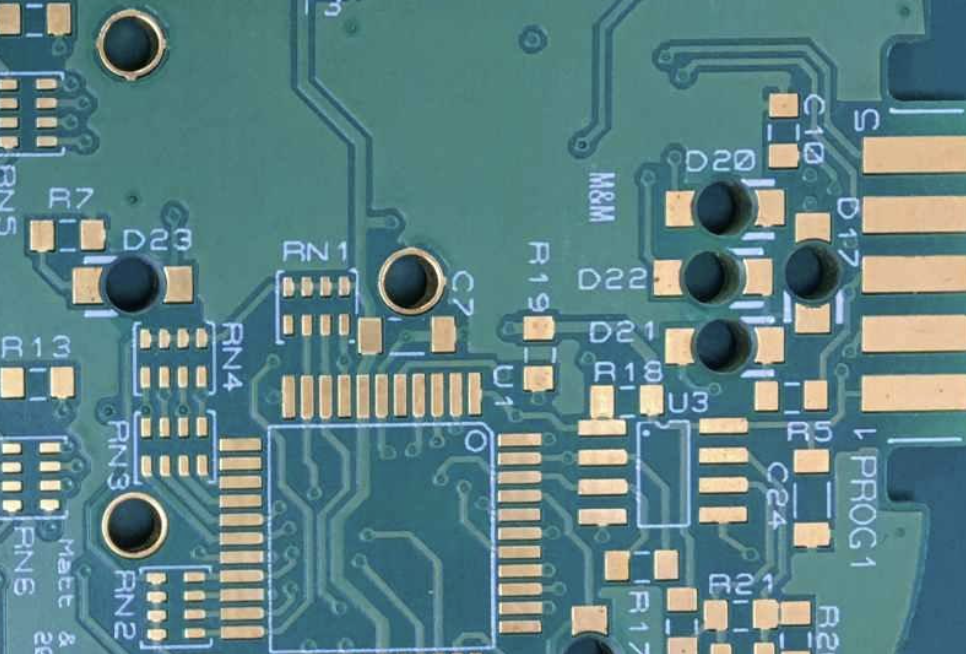

As a professional layout engineer, taking the time to organize the silkscreen properly is crucial. Here are 9 practical tips:
Fonts must be chosen based on available space, with the prerequisite that they "must be clearly readable." Common sizes are 35 mil height / 5 mil line width, and 25 mil height / 5 mil line width. It's best to confirm their process limits with your chosen board house during the design phase!
Be sure to mark component pins on the silkscreen. This is very helpful for later debugging and assembly. For example, mark Pin 4 on a ribbon cable connector, and ensure markings are present in dense pin areas like ICs or FPC connectors.
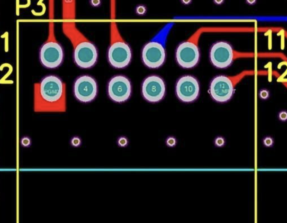
For ease of reading, it is recommended to keep silkscreen on the entire board in only two directions (left-to-right and bottom-to-top). Additionally, the reading direction of the silkscreen should preferably align with the usage direction of ICs, which can significantly reduce the chance of reverse soldering.

Following the previous point, please don't rotate silkscreen for small components like resistors and capacitors in all four directions. Otherwise, your eyes will get very tired turning the board around during维修 or debugging. Pro Tip: If components are too dense to place the reference designator, you can write the designator in a nearby blank area and draw a box with an arrow pointing to the component!
For polarized components like diodes and electrolytic capacitors, be sure to explicitly mark the direction on the silkscreen to minimize assembly errors. The direction and pin numbers for high-speed connectors should also be printed clearly to avoid reverse insertion.

All reference designators must be placed near their associated components. If the density is truly too high, they can be grouped together and marked with an arrow indicator.
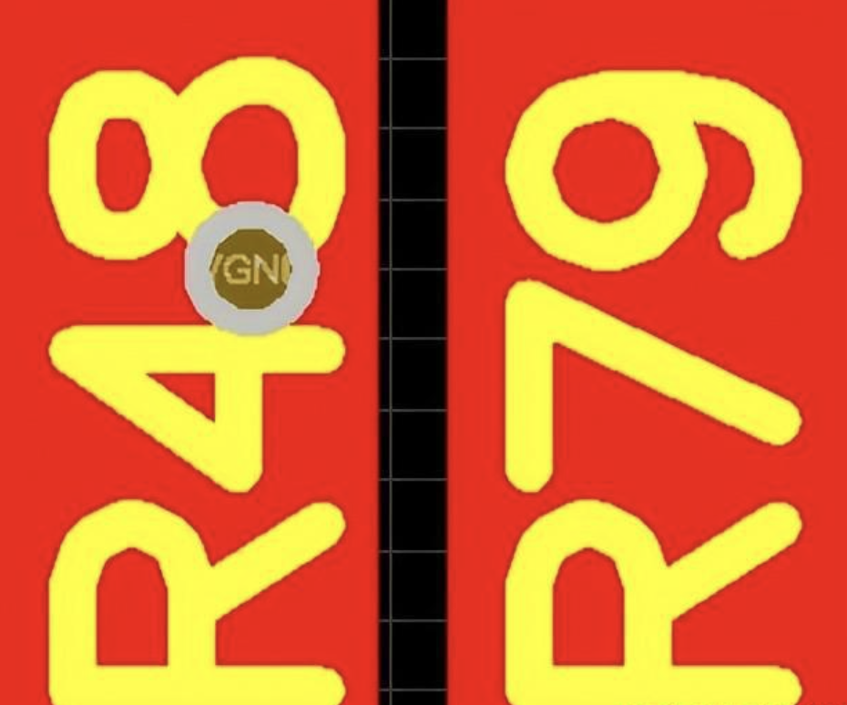
Absolutely do not place silkscreen text on component pads, as this will severely affect solderability! Also, if silkscreen is placed over vias, the text will be broken or missing on the fabricated board (e.g., if the number 8 is broken, you won't be able to tell if it's R48 or R49).
High-speed signal traces on the top or bottom layer can be considered microstrips. Placing silkscreen over these traces changes the dielectric constant in that area, leading to impedance discontinuity and affecting signal quality. (However, you don't need to worry about this for high-speed traces on inner layers!)
For special components with hidden leads underneath, like BGAs and QFNs, the silkscreen outline dimensions should ideally match the physical chip dimensions exactly. If drawn too large or too small, it can cause placement alignment issues and affect soldering yield.
We hope this technical compilation from eCloud helps you in your PCB design! For your specific PCB design project, do you need assistance compiling other specific layout guidelines (such as solder mask design or stack-up planning)?
