I. Definitions and Advantages of Blind and Buried Vias
Blind and buried vias provide electrical connections between board layers and are primary means for HDI technology to enhance signal density and PCB performance.
1. Definition and Functional Distinction
| Characteristic | Blind Via | Buried Via | Summary of Differences |
| :--- | :--- | :--- | :--- |
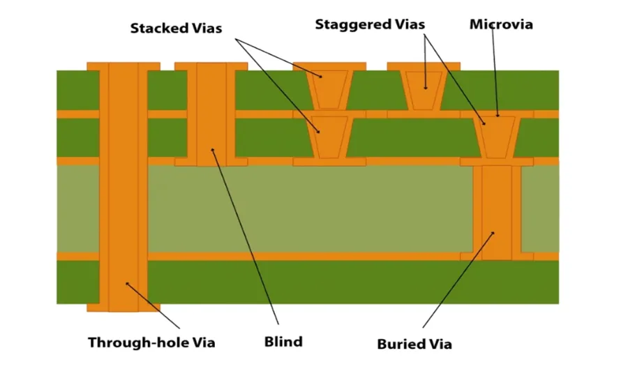
| Connected Layers | Connects an outer layer to one or more inner layers. | Connects two or more inner layers. | Blind vias occupy some outer layer space, while buried vias are completely hidden internally. |
| Visibility | Not visible from the opposite side of the PCB. | Completely hidden within the circuit board, invisible to the naked eye. | Buried vias do not occupy outer surface space, making them suitable for HDI boards where space is extremely critical. |
| Primary Purpose | Minimizes board area as they do not penetrate the entire PCB. | Used to meet high-density constraints for traces and pads without increasing the total layer count or board size. | |
2. Core Advantages of Blind and Buried Vias
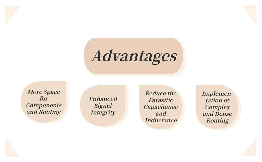
- Increase Signal Density and Performance: As key components of high-speed signal routing, blind/buried vias enable higher signal density than traditional PCBs, thereby improving signal quality and reducing crosstalk.
- Optimize Space and Layer Count: Help reduce PCB size and layer count because they can maintain functionality within smaller areas.
- Mechanical Stability: Blind vias can serve as mechanical stress relief points, especially in high-current applications. Current flowing through the via center reduces stress on the surface layers on both sides, preventing interlayer arcing.
- Improve Aspect Ratio: Blind and buried vias can help manage the printed circuit board's aspect ratio and limit variations in branching.
II. HDI PCB Layout Stack-up and Technology Levels
The technology level of an HDI board is often determined by the number of times blind vias are stacked.
1. HD Stack-up Types
HDI PCBs are generally fabricated using a build-up process. Common stack-up structures include:
- 1st-order HD: Typically has only one layer of blind vias.
- 2nd-order HD: Uses a process with more than one stack of blind vias.
- Any-layer Interconnect Board (Anylayer HDI): Every layer has stacked blind vias, representing the highest technology level.
Ideal stack-up examples for blind/buried vias include:
- 4-layer stack-up: 4 drilled layers, 1 blind or buried via layer, and 1 ground layer.
- 8-layer stack-up: 4 drilled layers and 4 blind or buried via layers.
- 10-layer stack-up: 5 drilled layers and 5 blind or buried via layers.
- 12-layer stack-up: 6 drilled layers and 6 blind or buried via layers.
2. Classification and Manufacturing Process of Blind Vias
Blind vias can be categorized by manufacturing process into mechanical blind vias, stacked blind vias, and staggered blind vias.
| Blind Via Classification | Connection Method & Manufacturing Technology | Characteristics |
| :--- | :--- | :--- |
| Mechanical Blind Via | Can be drilled using a standard drill press. | For example, a 6-layer PCB can have connections from L1 to L2, L1 to L3, etc. |
| Stacked Via | Blind vias on different layers are connected and stacked on top of each other. | Forms a blind via that penetrates multiple inner layers from the top layer, common in high-end HDI boards. |
| Staggered Via | Uses laser drilling; blind vias in different layers are not connected and are arranged in a staggered pattern. | Common in HDI circuit boards, offering higher routing density and flexibility. |

III. Best Practices and Considerations for Blind/Buried Via Layout
In HDI PCB layout, specific best practices must be followed to ensure manufacturing yield, signal integrity, and product reliability.
1. Via Usage Principles
- Minimize Length: Always strive to minimize the length of blind and buried vias to reduce the risk of damage caused by interlayer short circuits or poor routing.
- Use Single Paths: Use a single via wherever possible. Multiple blind or buried vias should only be used when necessary to reduce the risk of damage and short circuits during assembly.
- Match Trace Width: Use wider blind and buried vias whenever possible to ensure good electrical connection between copper layers. The required minimum trace width is typically 2 mils.
- Primarily for Signal Traces: Blind and buried vias are typically used for signal traces. If used for power lines or ground planes, ensure the correct impedance guidelines for each layer are followed.

2. Avoid High-Stress Areas
- Avoid High Thermal Expansion Areas: The coefficient of thermal expansion varies by material. It is essential to avoid placing blind and buried vias in areas with high thermal expansion or temperature cycling, as these conditions can create unnecessary stress, potentially leading to cracking or other issues later in the product's lifespan.
- Avoid Critical Paths: It is important not to place too many blind or buried vias in critical paths on the board, as this increases the risk of interlayer short circuits and significantly reduces yield.
3. Design Rules and Cost Considerations
- Correct Design Rules: Ensure your design rules accommodate both blind and buried vias to avoid any issues during manufacturing or testing.
- Cost and Complexity: PCBs using blind and buried vias remain more expensive to manufacture compared to those using standard through-hole vias. The higher cost is due to increased board complexity, additional steps in the manufacturing process, and the need for more frequent testing and precision checks.
Conclusion
HDI blind and buried via technology is the cornerstone for achieving the miniaturization and high performance of modern electronic devices. Although they increase the complexity of PCB design and manufacturing, careful planning, correct stack-up selection, and adherence to best practices—such as avoiding high-stress areas and minimizing via length—can significantly improve PCB reliability, signal integrity, and routing efficiency.
