I. What is a PCB Microvia?
Microvias are tiny holes used in PCBs to connect different layers. Their diameter typically ranges from 0.1 mm to 0.15 mm, with pad sizes generally less than 0.35 mm. Microvias help establish efficient signal and power paths in high-density PCBs. They increase the number of connections on a PCB without enlarging its size, which is crucial for meeting the demands of high-performance devices.
1. Core Advantages of Microvias
Using microvias in HDI PCBs offers multiple benefits, forming the cornerstone for achieving miniaturization and high performance.
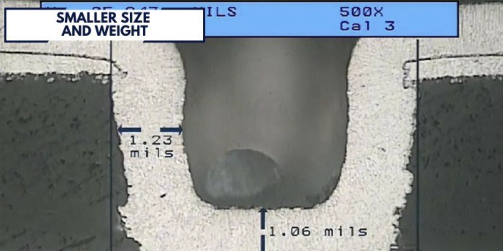
- Smaller Size, Lighter Weight: Microvias help reduce PCB size, making the board thinner, lighter, and easier to fit into smaller devices. This is especially important for devices like smartphones and laptops that must be lightweight and compact. The compact nature of microvias allows more components to be installed in the same area.
- Improved Performance: Being smaller than standard vias, microvias help shorten circuit paths on the PCB, enhancing overall circuit efficiency. They can increase transmission speeds and enable more accurate data transfer.
- Enhanced Signal Integrity: Microvias shorten signal communication paths, thereby improving overall signal communication and stability, particularly in 5G or high-speed applications. They can also reduce unwanted inductance and capacitance within the board structure, which can affect signal quality.
- Mechanical Stability: Evenly distributed microvias on a PCB can reduce damage caused by uneven stress. By providing stronger connections between layers, microvias improve the PCB's pressure resistance, ensuring it remains reliable even in harsh environments.
- Optimized Cost: Switching to microvias can reduce material waste, thereby lowering PCB costs. As microvias help reduce the number of layers, the design becomes simpler, streamlining the assembly process and improving overall efficiency. This leads to lower total costs, especially in mass production scenarios.
II. Types and Manufacturing Processes of Microvias
Microvias can be categorized into different types based on design requirements. Understanding these types is crucial for optimizing HDI PCB design.
1. Types of Microvias
| Microvia Type | Definition & Connection Method | Key Advantages |
| :--- | :--- | :--- |
| Buried Via | Used to connect inner layers of an HDI PCB, completely encapsulated within the inner layers. | Enables miniaturized circuit boards, provides greater routing space on the surface. Reduces signal loss (e.g., EMI interference) and enhances the overall performance of the PCB. |
| Blind Via | Interconnects an outer layer of the PCB with an inner layer but is not a through-hole. | Saves space; similar to buried vias, offers a range of advantages for enhancing signal integrity. |
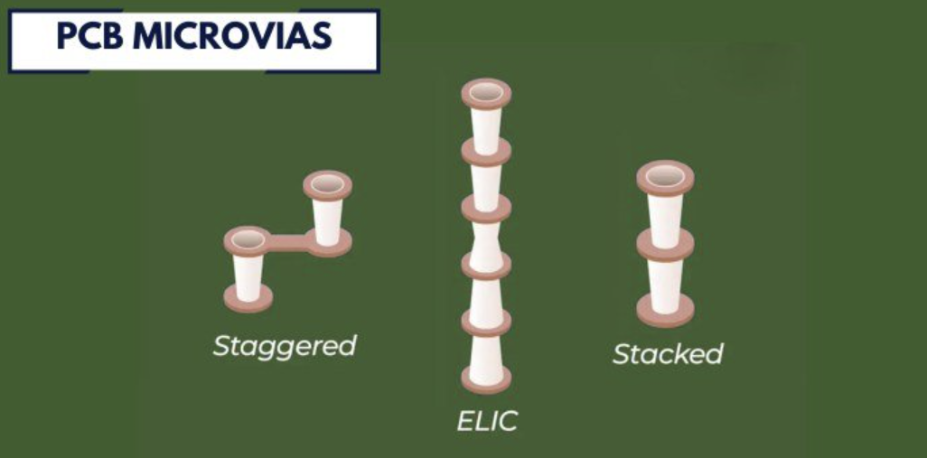
| Stacked Via | Microvias stacked layer upon layer, used to connect different layers within the PCB. Typically filled with copper to ensure conductivity and strength. | Enables complex and space-saving multi-layer designs, providing greater design flexibility. |
| Staggered Via | Microvias arranged in a non-linear, staggered pattern relative to each other. | Minimizes the possibility of delamination, enhancing the PCB's mechanical stability. The staggered layout helps distribute stress during the assembly process. |

2. Manufacturing Process of Microvias
Microvias are typically manufactured using laser drilling, allowing for the creation of space-saving and reliable circuit boards. Microvias can also be of different types such as blind, buried, or stacked vias.
III. Challenges and Considerations in Microvia Design
When designing HDI PCBs with microvias, certain challenges must be carefully addressed, as they can affect the PCB's performance and reliability.
1. Aspect Ratio Control
The aspect ratio in microvia design refers to the ratio of the microvia's depth to its diameter.
- Problem: An excessively high aspect ratio can lead to issues like cracking, poor copper plating, or mechanical stress.
- Standard: The aspect ratio must be limited to avoid these problems. According to IPC standards, the ideal aspect ratio is 1:1. The correct aspect ratio ensures higher reliability and a longer lifespan.
2. Thermal Management
Thermal management is critical for HDI PCBs, especially when using microvias.
- Problem: Tightly packed component layouts generate heat, and microvias can become sources of heat generation, leading to stress and damage in the PCB.
- Solution: Appropriate PCB materials must be used, and thermal vias should be incorporated. Installing heatsinks also aids in heat dissipation for optimal performance.
3. Material Selection
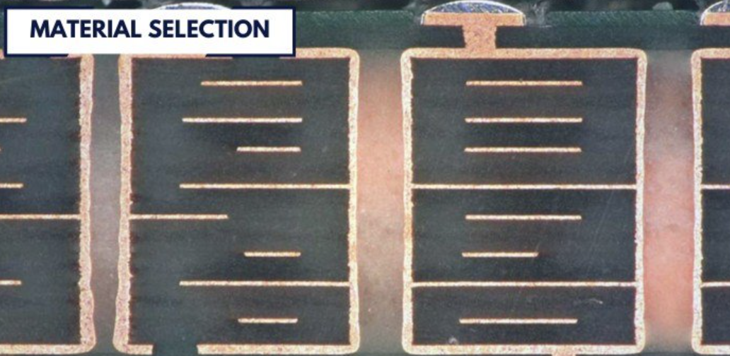
Materials must be carefully chosen for HDI PCBs utilizing microvias. Since microvias are processed by laser, the selected materials should possess good thermal and electrical properties.
- Ceramic-filled PTFE (e.g., Rogers RO3003): Features extremely low dielectric loss (Df approx. 0.0013 to 0.004) and good thermal conductivity, making it highly suitable for RF applications like 5G antennas and microwave waveguides.
- Low Thermal Expansion Ceramic Composite (e.g., Panasonic Megtron 6): Features very low CTE (Coefficient of Thermal Expansion) and a Dk of approx. 2.6 to 2.7, making it very suitable for high-reliability multi-layer HDI structures.
4. Via Type and HDI Stack-up Design
- The choice of via type depends on the specific application. Stacked vias save space but are more complex and costly to manufacture. Staggered vias offer better mechanical stability.
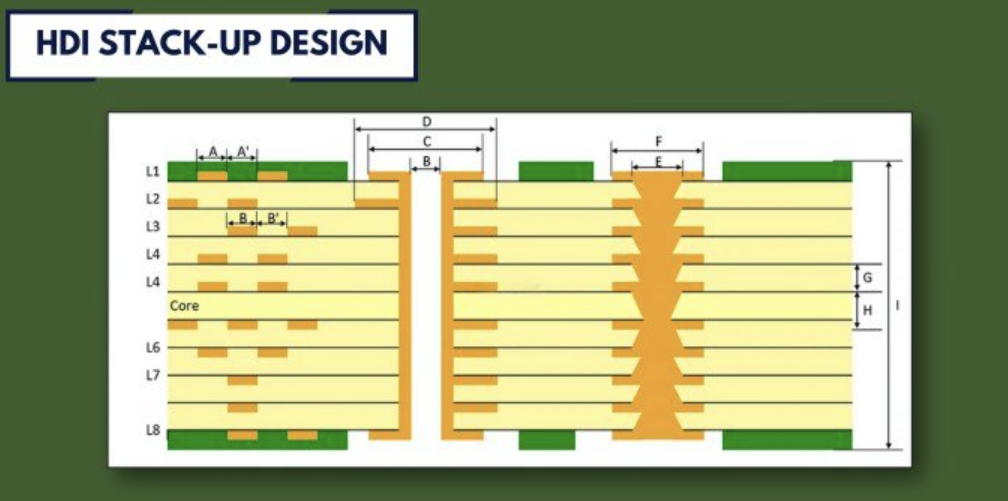
- The design of the HDI stack-up is crucial for the proper functioning of microvias. Microvias must be selected for the different layers in the stack-up to meet requirements. Layer thickness, dielectric material quality, and the number of microvias are primary considerations.
IV. When Should Microvia Technology Be Adopted?
Microvias help save space and enhance PCB design, but they also increase cost and manufacturing complexity. You must weigh when it's necessary to use them in your design.
1. Scenarios Suitable for Microvias
- High-Density BGA Layouts: When the density requirements of BGAs make standard vias insufficient for routing, especially when ball pitch is limited. Microvia structures often follow the BGA pattern, connecting BGA pads to increase density while maintaining performance.
- Reducing Via Size: By decreasing via pad sizes, the spacing between functional components can be made more compact. This frees up space between component arrangements where channels previously could not exist.
- Improving Electrical Performance: Microvias can eliminate obstructions in power and ground layers, thereby reducing inductance and hotspots. Staggered vias can move drill locations away from pads, alleviating congestion.
2. Difference Between Microvias and Through-Holes (Common Questions)
- Microvias are small, dense holes located within the board's interior, used to connect adjacent layers and are suitable for high-density designs.
- Blind and Buried Vias are also suitable for high-density designs.
- Standard Through-Holes (PTH) are located at the top or bottom of the board and penetrate all layers.
3. Determining Microvia Size
Microvia size depends on the aspect ratio, dielectric layer thickness, and pad size. The size calculation method is as follows:
- Select the required HDI stack-up.
- Determine the maximum drill bit size for the tightest routing area.
- Calculate the required layer thickness.
- Select a laser-drillable prepreg that meets the thickness.
- Verify that the microvia meets aspect ratio limits and material requirements.
Conclusion
For HDI PCBs, microvias help save space, enhance design performance, and improve PCB reliability. However, numerous challenges exist regarding microvia size, materials used, and thermal management. Designing an appropriate via structure and stack-up can help you fully leverage the advantages of microvias while avoiding potential problems.
