I. Core Definition of Tiers: Judging by the "Hole"
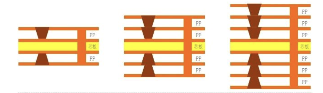
The core basis for distinguishing HDI board tiers is not the total board thickness, but rather the number of inner layers spanned by the blind vias and the number of lamination and laser drilling cycles.
- First Tier: Blind vias connect only the surface layer to the adjacent first inner layer.
- Second Tier: Blind vias can connect to the second inner layer (achieved through stacking or staggering two layers of blind vias).
- High Tier (Third and above): Blind vias can extend to the third or deeper inner layers, with a multi-level via structure configuration.
Each increase in tier means adding one more lamination (build-up) cycle and one more laser drilling process in the manufacturing sequence.
II. Detailed Breakdown of Each HDI Tier: From Express Lane to 3D Hub
1. First-Tier HDI: The Intuitive and Efficient Entry Point
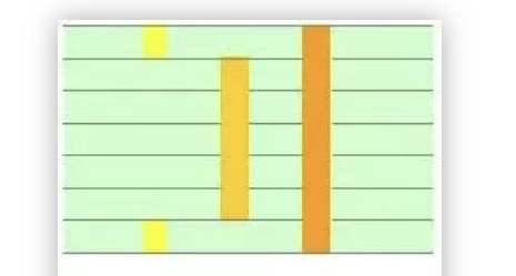
- Process Characteristic: Employs a "one lamination + one laser drilling" process. For example, in a 6-layer first-tier board, blind vias exist only between L1-L2 and L5-L6, with connections in the middle made through plated through-holes or buried vias. This is also known as the "1+N+1" structure.
- Technical Analogy: Like a single-track subway line—simple paths, clear efficiency.
- Application Scenarios: Suitable for products with some space constraints but not extremely high overall signal density. Examples: simple modules in smartphones, Bluetooth earbuds.
- Typical Case: The charging case control board for a brand's TWS true wireless earbuds uses a first-tier HDI design. While ensuring signal integrity, it successfully controls the board thickness to 0.6 mm.
- Advantages/Disadvantages: Low cost, easy process control, but limited interlayer interconnection capability, unable to handle extremely high-density routing.
2. Second-Tier HDI: The Core of 3D Routing with Stacked and Staggered Vias
- Process Characteristic: Employs "two lamination + two laser drilling" cycles. It contains two microvia levels, achieving interlayer connections through "stacked vias" (via on via) or "staggered vias" (offset via positions). This is known as the "2+N+2" structure.
- Technical Analogy: Like a multi-level interchange, significantly increasing routing freedom.
- Manufacturing Challenges (Hidden Thresholds):
- Alignment Deviation: A contract manufacturing case showed that a mere 0.05 mm layer-to-layer misalignment (about half the thickness of a human hair) could reduce the yield of second-tier HDI boards to below 75%.
- Plated Copper Uniformity: The BMS control board for an EV manufacturer once failed a 120°C high-temperature test due to thermal expansion, caused by a ~3 μm variation in buried via copper thickness.
- Application Scenarios: High-end smartphones, tablets, 5G base station main control boards.
- Actual Case: A domestic foldable smartphone integrates a 5G RF module and display driver circuitry into an area the size of a fingernail using an 8-layer second-tier HDI board.

3. Third-Tier and Higher HDI: The Extreme Challenge of Micron-Level Processes
- Process Characteristic: Employs "three lamination + multiple laser drilling" cycles or more complex sequential lamination processes. This can even extend to Any-layer Interconnect (Any-layer HDI / ELIC).
- Technical Analogy: The "micro-carving art" of PCB manufacturing, requiring precise hole formation at ~10 μm level accuracy.
- Equipment Threshold: For instance, a medical ultrasound probe project required a hole diameter tolerance of ±5 μm (equivalent to an error of no more than 1 cm over 100 meters), necessitating the introduction of femtosecond laser equipment. While this can improve process efficiency by about 40%, the investment for a single machine is substantial, putting it out of reach for most small to medium-sized board shops.
- Application Scenarios: Autonomous driving, satellite communications, military radar, ultra-precision medical instruments.
- Typical Case: The autonomous driving control module for a German automaker uses a 16-layer third-tier HDI board with over 2,000 laser microvias on the board to ensure real-time transmission of millimeter-wave radar signals.

III. The Key Decision: Trading Off Between Cost and Performance
Choosing the HDI tier isn't about "the higher, the better." It requires precise "calculation" based on the specific scenario. The following three real-world cases illustrate the selection logic in different fields:
1. Consumer Electronics: Cost Takes Priority
At a mobile phone assembly factory, engineers compared two options: a 10-layer second-tier board vs. a 10-layer third-tier board. Although the third-tier design could reduce volume by an additional 8%, the cost increased by about 30%. For a mass-produced product, the space advantage did not outweigh the cost increase, leading to the final choice of the second-tier solution.
2. Automotive Electronics: Paying for Reliability
A startup car manufacturer's domain controller originally used a 6-layer first-tier HDI but exhibited impedance anomalies during –40°C low-temperature testing. After upgrading to a third-tier HDI combined with embedded capacitor design, the temperature drift was reduced by about 70%. Although the cost per board increased by 45%, it avoided the risk of a full vehicle recall, making it a necessary upgrade.
3. Military/Aerospace: Higher Tier Doesn't Equal Optimal
A satellite communication device was originally designed with a third-tier HDI. However, vacuum testing revealed that the laser via taper angle affected signal reflection. The final solution was to revert to a second-tier stacked via structure and adjust the dielectric dissipation factor (Df) to 0.002, successfully resolving the issue. The key lies in the combination of material and tier, not blindly pursuing a higher tier.
IV. Conclusion
The tier classification of HDI boards, from the entry-level first tier to the third tier, reflects the electronics industry's relentless challenge of "extreme manufacturing."
- First Tier offers high cost-performance, suitable for most mainstream consumer electronics.
- Second Tier is the current mainstream for high-end products, balancing density and cost.
- Third Tier and above are born for extreme applications like aerospace, medical, and military uses.
A mature engineering decision is never about choosing the "highest tier," but rather the "most appropriate tier."
In the world of micron-level manufacturing, true technical wisdom is often demonstrated by knowing when to stop at the mature stability of the second tier and when it is necessary to challenge the limits of the third.
