June 11, 2026
COMPUTEX 2026 has just concluded, and the figures Jensen Huang dropped while unveiling the Vera Rubin platform at GTC Taipei shocked the entire industry: a single architecture utilizing nearly 2 million components, over 150 Taiwanese supply chain partners, and a 10x improvement in inference performance per watt. However, hidden behind these glamorous numbers is a crisis in packaging substrates for AI servers.
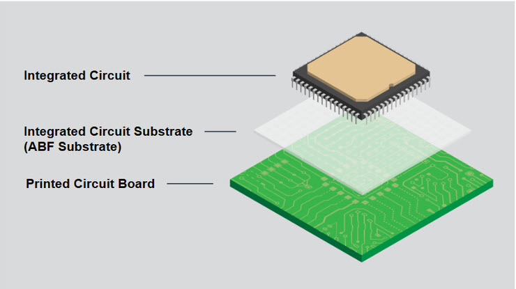
Coupled with Rubin's comprehensive shift to liquid cooling and the continuous rise in single‑rack power consumption, the CTE, rigidity, and thermal compatibility of traditional ABF (Ajinomoto Build‑up Film) substrates are approaching the physical limits of the material. This is why Intel is willing to invest over $1 billion and accumulate nearly 600 patents in glass substrate R&D—the packaging battlefield of the next decade has officially expanded from organic substrates to glass cores.
According to an inventory published by TechSearch International at BUSS'25, there are currently at least 14 companies globally investing in glass core R&D. The list spans IDMs, traditional substrate manufacturers, OSATs, and material suppliers: Intel, Absolics, AT&S, Dai Nippon Printing, FICT, Ibiden, LG Innotek, Qorvo, Samtec, SEMCO, Shinko Electric, Sony, Toppan, as well as Taiwan's Unimicron. The entire semiconductor packaging supply chain is almost collectively placing its bets.
None of the challenges the industry currently faces are easy to solve:
Glass substrates will not replace ABF overnight, but the signals revealed at COMPUTEX 2026 are quite clear—top‑tier applications will be the first beachhead for glass.
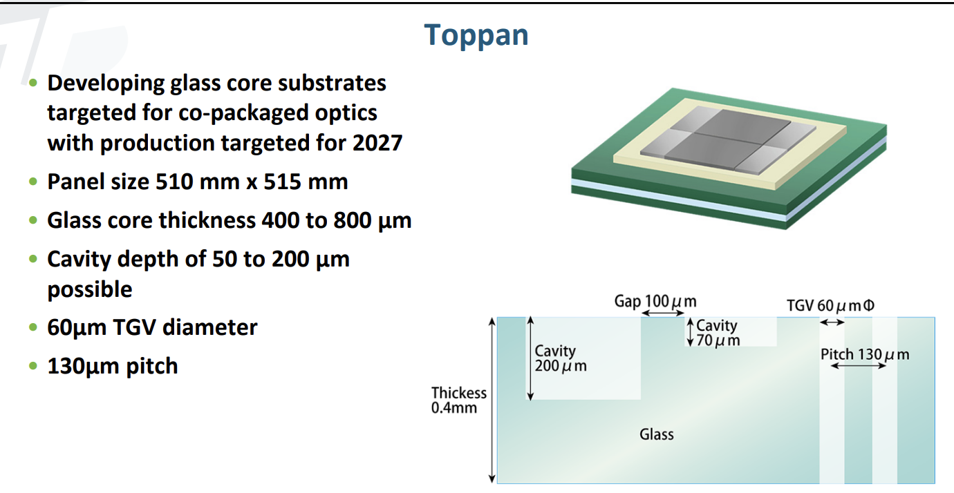
Toppan has publicly planned to mass‑produce 510mm × 515mm glass core substrates in 2027, targeting CPO applications. The glass core will have a thickness of 400–800µm, a TGV diameter of 60µm, a pitch of 130µm, and support a 50–200µm cavity structure to accommodate optical components. NVIDIA's Spectrum‑X Photonics, announced at this COMPUTEX, is the world's first mass‑produced 200Gb/s SerDes Ethernet switch, with CoreWeave, Lambda, and Oracle Cloud as early adopters. The advantages of glass substrates in high frequency, low loss, and optoelectronic integration perfectly match the appetite of CPO.
Intel's EMIB‑T has planned a maximum packaging size of 120mm × 180mm, capable of stacking over 24 HBMs; TSMC's CoWoS roadmap points to a 9.5X reticle and a 120mm × 150mm substrate. At these ultra‑large sizes, the warpage and yield issues of ABF substrates become even more acute, amplifying the rigidity advantage of glass cores.
| Timeframe | Mainstream Structure | Role of Glass Core | | :--- | :--- | :--- | | Short‑term (2026–2028) | ABF‑dominated | Pilot production, premium small‑volume adoption | | Mid‑term (2028–2032) | Coexistence of ABF and Glass | Entry into CPO and premium AI packaging | | Long‑term (2032+) | Divergence of two paths | Firmly established in highest‑end products |
It is worth noting that Ajinomoto's new ABF plant will not begin production until 2032—in other words, the maturity timeline for glass substrates perfectly aligns right before ABF capacity catches up. These six years will be the most intensely competitive stage for the two technologies.
For R&D engineers and procurement managers, what must be avoided right now is treating glass substrates as the next hot thing that “will be ubiquitous next year,” or conversely thinking that “glass is too far off to care about.” This is a long‑term transition between 2026 and 2032: ABF will still shoulder the vast majority of AI server packaging shipment volumes, while glass cores will first make inroads into CPO, top‑tier HPC, and optoelectronic integration. True competitiveness lies in simultaneously mastering the build‑up design, impedance control, reliability verification, and prototyping pacing of both routes.
eCloud Technology's core positioning is to connect clients with the most suitable manufacturing partners and material selections for frontier applications such as HDI, high‑speed networking, silicon photonics, and high‑frequency RF. If your next‑generation product is facing challenges with large‑size substrate yields, fine‑line build‑ups, CPO optoelectronic integration, or specialized material prototyping, we welcome you to contact our engineering team—let's work together to turn the possibilities on the spec sheet into a mass‑producible reality.
Sources: TechSearch International, Inc. IEEE BUSS'25 Report; NVIDIA GTC Taipei @ COMPUTEX 2026 keynote; Ajinomoto Co., Inc. May 2026 announcement. This article is for technical exchange and reference only and does not constitute investment advice.
