Why is HDI DFM Harder Than Standard PCBs?
For traditional 4- or 6-layer boards, DFM mostly involves checking basic constraints like trace width and spacing, annular rings, and drill registration. But HDI design constraints operate on a completely different scale:
- High signal density: BGA pitches are squeezed from 0.8 mm down to 0.4 mm or even smaller, making routing space extremely tight.
- Narrow routing channels: The escape routing space between pads often only allows for 1 to 2 trace widths.
- Extreme layer‑to‑layer registration demands: In the sequential build‑up process, every additional lamination accumulates registration error, and the yield curve can drop by an entire order of magnitude.
- Shrinking component footprints: Standard routing techniques (like dog‑boning) simply don’t fit at small pitches, forcing designers to use via‑in‑pad.
When CAM engineers receive Gerber/ODB++/IPC‑2581 files, they run a DFM check to compare your design against the factory’s mass‑production capabilities (trace‑to‑trace, via diameter, annular ring, etc.). If you fail this check and force it into production anyway, the consequences are typically scrapped materials, delayed lead times, and halted customer production lines. Hit all three, and the BU’s quarterly numbers will look terrible.
Three Major Manufacturing Challenges: Understand What the Fab is Afraid Of
To make the right DFM decisions, engineers must first understand the fab’s biggest pain points in the HDI process.
Challenge 1: Fine Lines and Spaces – A Tug‑of‑War with Physical Limits
To produce stable traces under 3 mil, the factory must simultaneously control exposure resolution, layer registration, and etching uniformity, all while operating in a highly controlled cleanroom environment.
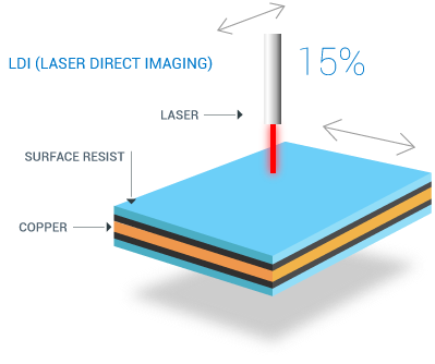
- Insufficient image resolution blurs fine lines: Traditional film exposure easily causes edge distortion on fine traces. Most mid‑to‑high‑end fabs have switched to LDI (Laser Direct Imaging), which uses computer‑controlled laser beams to write patterns directly. This drastically improves resolution, results in cleaner photoresist development, and effectively suppresses etchant side‑seepage.
- Etch undercut turns traces into trapezoids: The thicker the copper, the longer the etching time, and the worse the undercut. Ultimately, the trace cross‑section becomes a trapezoid (narrow on top, wide on the bottom), which is a massive taboo for impedance matching. In practice, HDI fine lines often use ½ oz, ⅓ oz, or even ¼ oz thin copper to prioritise trace geometry precision.

- Dust contamination instantly breaks 1 mil traces: When trace widths shrink to the 1 mil level, a single hair or dust particle can cause an open or short circuit. Fabs must use an ISO 14644‑1 Class 100 cleanroom. You are paying for that environmental control cost, which is why HDI boards are priced a tier higher.
Challenge 2: Small Vias Under 6 Mil – Hard to Drill, Hard to Plate
Shrinking via diameters is the most direct way to increase routing density, but machining small holes is far more complex than designers imagine.
- Under 6 mil requires lasers: Mechanical drill bits under 6 mil lack the rigidity to withstand cutting forces, causing breakage rates to spike. HDI microvias mostly use laser drilling to control depth precision. The rule of thumb is that the laser‑drilled via diameter should be about 1.3 × the dielectric thickness.
- Aspect Ratio is the life‑or‑death line for microvias: The deeper and narrower the hole, the harder it is for copper plating solutions to circulate. Microvia aspect ratios must be kept under 0.75:1. Exceeding this causes plating uniformity to collapse, leading to failures in reliability testing (IST, thermal cycling).
- Dielectric layers must be uniform: Traditional FR‑4 is a composite of resin and fibreglass. Their differing laser absorption rates cause uneven hole walls. Opting for finer‑weave fibreglass or non‑woven reinforcements (like PTFE or aramid) significantly improves hole wall quality.
- Thermal stability hurdles for ultra‑thin dielectrics: To control the aspect ratio, dielectrics must be thinner, sometimes requiring unreinforced materials (like epoxy liquid, polyimide, or RCC) to go as thin as 1 mil. However, these materials are sensitive to thermal deformation, meaning lamination and reflow temperature profiles must be re‑evaluated.
- The Via‑in‑Pad dilemma: When BGA pitches drop below 0.5 mm, via‑in‑pad becomes the only option. While it offers “zero‑cost escape routing”, it requires additional drilling, plating, plugging, and capping. This increases costs, lengthens lead times, and severely tests the fab’s planarisation control. Only use via‑in‑pad when routing is truly impossible otherwise.
Challenge 3: Interlayer Connection Flexibility – The True Watershed of HDI
The essence of HDI is connecting only the layers that need it, but this brings massive complexity to lamination and via structures.
- Blind via limitations: Blind vias generally only span up to 3 layers. An HDI stack‑up practically maxes out at 3 laminations (1+N+1, 2+N+2, Any‑Layer). Anything more causes cumulative registration errors to explode.
- Stacked via vs. Staggered via – always prioritise staggered: Stacking microvias directly requires every layer to undergo plugging and planarisation, which skyrockets costs and increases the risk of voids. Prioritise staggered (offset) structures, which skip planarisation, offer higher reliability, and cost less.
- Any‑Layer architecture costs: An all‑microvia Any‑Layer structure offers maximum routing freedom, but every sequential build‑up is another press‑drill‑plate cycle. The total cost can be 3 to 5 times higher than a traditional through‑hole board.
5 DFM Decisions Engineers Must Make Before Sending Samples
Internalise the process constraints above and finalise these key decisions during the layout phase.
1. Via Structure Priority: Staggered > Stacked
Unless stacking is absolutely mandatory, staggered configurations are always the top choice. They bypass planarisation, lower the risk of voids, and offer superior mechanical and thermal reliability.
2. Annular Ring Must Be At Least 2 mil (0.05 mm)
An undersized annular ring will easily crack or break out under stress.
- Microvia annular ring ≥ 0.05 mm (2 mil).
- Outer layer isolated area reduction (due to defects) ≤ 20%.
- Inner layer isolated area reduction (due to pits/pinholes) ≤ 25 μm (1 mil).
- IPC Class 3 applications should push for 4 mil or more for extra margin.
3. Surface Finish: ENIG or ENEPIG for Fine Pitch BGAs
The planarity and solderability of the surface finish directly determine SMT yield for HDI boards.
- ENIG (Electroless Nickel Immersion Gold): Recommended for fine‑pitch BGAs, offering great planarity and consistency.
- ENEPIG (Electroless Nickel Electroless Palladium Immersion Gold): Adds a palladium layer for better SMT shear strength and wire‑bonding suitability, though it costs more.
- Other finishes (OSP, Immersion Silver, Hard Gold) should be evaluated strictly based on application scenarios.
4. Aspect Ratios: Know Your Baselines
- Through‑hole AR limit is 10:1 (Board Thickness / Minimum Hole Diameter).
- Microvia AR limit is 0.75:1 (Drill Depth / Minimum Hole Diameter).
Calculate these during design; don’t wait for the CAM engineer to flag them.
5. Material Selection: Tg ≥ 200 °C for High‑Reliability
- Tg ≥ 200 °C prevents board degradation after multiple laminations and reflows.
- High Td & high thermal conductivity preserve operating windows and aid heat dissipation.
- Laser drilling compatibility – must stably drill down to 4 mil without excessive carbonisation.
Common material families include TU‑863+, Isola 370HR, Ventec VT47, and Rogers RO4003/RO4350.
High‑End Applications: Positive Etchback and Class 3 Standards
If your board targets military, aerospace, automotive ADAS, or medical markets, include these details in your fab notes.
Positive Etchback is More Reliable
- Negative etchback applies a protective layer before etching exposed copper, resulting in weaker connection points.
- Positive etchback plates the copper first and then selectively etches it, forming a much more reliable three‑point connection.
Example Fab Note:
“Apply positive etchback per IPC‑6012 Class 3. Copper land protrusion must be visible after desmear.”
Class 3 Related Standards List
Ensure your fab has relevant certifications like IPC Class 3/3A, AS9100D, MIL‑PRF‑55110, or MIL‑PRF‑31032. Proactively request and explicitly list required documents on your PO, such as the Certificate of Conformance (CoC), material specs, First Article Inspection Report, and ionic contamination test reports.
Editor’s Conclusion
HDI DFM might seem like an endless list of rules, but what truly separates engineering tiers is making the right judgments before design – not scrambling to fix things after CAM rejects it.
- DFM is the designer’s responsibility: The fab can only point out minimum capabilities; they cannot recover your lost schedule or material costs.
- The three HDI bottlenecks: Fine‑line etching, microvia drilling/plating, and interlayer structures dictate yield and cost.
- Design priorities: Choose staggered over stacked, dogbone over via‑in‑pad, and minimise lamination cycles over forcing Any‑Layer.
- Memorise the metrics: Annular ring ≥ 2 mil, microvia AR ≤ 0.75:1, through‑hole AR ≤ 10:1, Tg ≥ 200 °C.
There are no shortcuts in HDI design. By internalising DFM thinking into every layout decision, you ensure your R&D efforts actually result in a stable, shipping product – not just a pretty Gerber file stuck in the prototyping phase.
