June 10, 2026
Whenever you're mapping out the stackup for a new project, do you often get stuck on these questions? ●"Does this BGA really need HDI?" ●"The fab replied with 2+N+2, is that the same as IPC Type III?" ●"The client wants to cut costs, but engineers are worried about signal integrity—should we add more layers?" These aren't technical problems; they are decision-making problems. This article cuts straight to the chase, helping you clarify the three key decisions of HDI stackup design in under 3 minutes.

Many people rely on experience to guess, but there are actually very clear indicators.
Look directly at the main IC's BGA pitch:
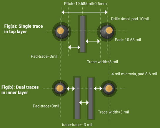
Next, look at the BGA breakout layer requirements:
Ironclad rule: As long as the design requires microvia‑based via‑in‑pad, regardless of your net count or how fast the speeds are, HDI is a necessary choice – no exceptions.
Stop using “the speed isn’t that fast” as an excuse to reject HDI. The true anchors for this decision are always the package pitch and breakout density.
This is something many R&D engineers misunderstand. HDI stackups have two parallel classification systems, and you must know how to use both.
Practical application guide:
| Scenario | Which system to use | | :--- | :--- | | Writing spec sheets, handling compliance documents | IPC‑2226 Type classification | | Getting quotes from fabs, comparing stackup costs | i+N+i notation |
If you cannot seamlessly switch between these two languages, your communication efficiency with the fab will drop by half.
The most common engineering disaster in HDI stackups isn’t under‑design – it’s over‑design. Every additional sequential lamination cycle adds yield risks and costs.
The rule isn’t “use stacked microvias whenever possible”. The priority should be:
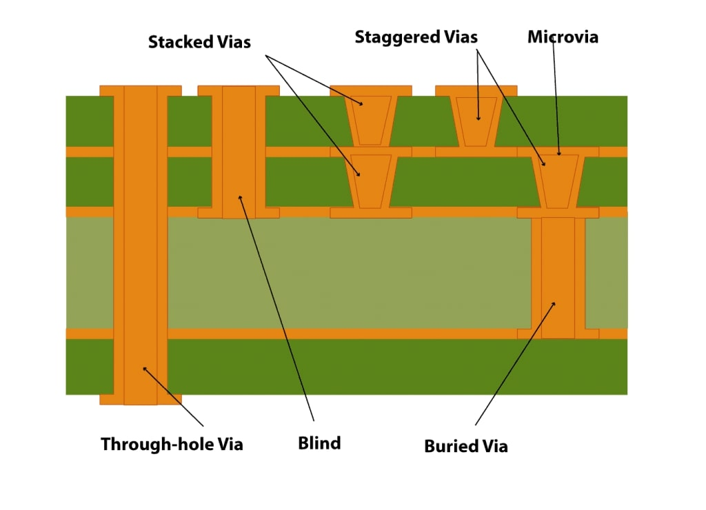
Prepreg thickness tolerances are usually ±10–15%. Factor this variation into your impedance calculations – don’t just force a single, rigid value.
Waiting until the Layout phase to go back and revise the stackup will double your costs. Evaluate HDI needs simultaneously while selecting ICs.
The manufacturability of the i+N+i structure, microvia aspect ratios, and the fab’s material library support are all key to stackup success. Align on these before the Schematic is even completed.
Over‑design won’t make your board more reliable; it will only increase BOM costs and extend prototyping lead times. Achieving design goals with the simplest architecture is what engineers should always strive for.
There is no universal solution for HDI stackup design. The entire process is a trade‑off across five dimensions: routing density, signal integrity, PDN performance, fab capabilities, and cost.
As long as you internalise the three key decisions above into your SOP, you can avoid 80% of stackup mistakes.
If your project is currently facing challenges with fine‑pitch BGA breakouts, HDI stackup selection, or impedance simulation verification, it is highly recommended to connect with an integrated service provider equipped with HDI engineering capabilities before prototyping. Addressing engineering risks upfront will make the path from prototype to mass production significantly smoother.
