June 12, 2026
This article analyses the transition zone—the most vulnerable area in Rigid-Flex designs—and outlines four critical design pitfalls that RDs must avoid.


Design Guidelines Summary Table
| Design Feature | Conventional Rigid PCB Practice | DFM Specification for Rigid-Flex Transition & Flex Zone | Physical Mechanism & Failure Prevention | | :--- | :--- | :--- | :--- | | Trace Direction & Corners | 45° routing or arbitrary angles allowed, often with corners | Must be perpendicular to the bend line, only smooth curves allowed | Avoid shear stress concentration and copper foil edge tearing | | Multi-layer Routing Alignment | Traces on different layers often stacked vertically for density | Mandate Staggered Routing | Eliminate the "I-Beam" effect, ensure flex zone柔韧性 | | Via Placement | Placed arbitrarily based on electrical needs, via-in-pad common | Strictly prohibited in the transition zone; distance from junction >1.25mm | Prevent rigid plated via barrels from cracking due to拉扯 during bending | | Ground Plane Design | Large area Solid copper pour | Must use Cross-hatched pour | Reduce overall rigidity, improve mechanical fatigue resistance | | Fine Traces & Protection | Pursuing minimum trace width, placed on any signal layer | Traces < 10 mils should be placed near the Neutral Axis | Keep脆弱 traces in a zero-stress zone, prevent outer拉伸断裂 |
The challenges of the transition zone exist not only in the X-Y plane trace layout but also in the Z-axis Stack-up Design, which determines the board's viability. R&D must master the following three key points:
While R&D diligently follows the Flex PCB design rules above, they must also calculate the bend radius early in the design process to address mechanical interference. IPC-2223 recommends the limit formula for safe bending:
Formula: $$R = k \times \text{Board Thickness}$$
Application of k Value:
| Bend Type | Definition | Recommended k Value | | :--- | :--- | :--- | | Static Flex | Bent only once or twice during assembly (e.g., inside a sensor) | 6 - 10 | | Dynamic Flex | Subjected to thousands or millions of flex cycles (e.g., foldable device hinge) | 10 - 20 |
Calculation Example: Assume a flex board stack-up has a total thickness = 0.0108 inches. If the application is Static flex (take k = 10), the minimum Bend Radius is: R = 10 × 0.0108 = 0.108 inches
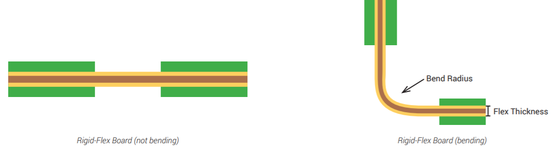 If a mechanical engineer, pursuing extreme thinness, forcibly compresses the transition zone below this radius, even the most perfectly designed traces by R&D will fail during reliability testing.
Rigid-Flex PCB technology is the ultimate weapon for product miniaturization, but the Transition Zone is also the zone that destroys yields. From avoiding parallel traces and implementing staggered layouts to adopting cross-hatched copper pours and bikini build coverlay processes, every guideline is a hard-earned lesson from countless failure analyses.
If your team is developing a Rigid-Flex PCB, eCloud can provide a DFM Review during the Layout phase to help avoid transition zone cracks and manufacturing failures. Feel free to contact us to ensure your project successfully progresses to mass production!
