December 19, 2025
Over the past few years, as the wave of artificial intelligence (AI) swept across the globe, TSMC's CoWoS (Chip-on-Wafer-on-Substrate) technology rapidly became synonymous with the advanced packaging field. This was due to its perfect alignment with AI chips' demands for high computing power and performance. However, a recently leaked internal report from NVIDIA has thrust a new technology called “CoWoP” into the spotlight. This technology claims to eliminate the need for expensive packaging substrates, sparking intense debate over whether it could challenge CoWoS's dominant position.
Is CoWoP just a flash-in-the-pan topic for hype, or is it a disruptive force powerful enough to rewrite the semiconductor and PCB landscape? This article will take you deep into the analysis of this new battle in advanced packaging.
Before discussing the challenger, we must first understand the current champion—CoWoS.
CoWoS stands for Chip-on-Wafer-on-Substrate, a 2.5D advanced packaging technology introduced by TSMC. It is called "advanced packaging" because it breaks through the limitations of traditional packaging, which places chips individually on a circuit board.
The core structure of CoWoS can be imagined as a "three-layer sandwich":
Simply put, the CoWoS path is: Chip → Silicon Interposer → Packaging Substrate → PCB Motherboard. It is precisely because of this middle "silicon interposer" layer that CoWoS can significantly shorten the distance between chips, enhancing computing performance, making it the standard for top-tier AI chips like the NVIDIA H100 and AMD MI300.
(Schematic of CoWoS Structure: Top to Bottom) GPU + HBM (Chip) | Silicon Interposer (Interposer) | Packaging Substrate (Substrate) + BGA | PCB Motherboard
CoWoP stands for Chip-on-Wafer-on-PCB. The biggest selling point of this technology is "subtraction": it attempts to omit the expensive "packaging substrate" (like ABF or BT substrates) and "BGA" (Ball Grid Array) solder balls from the CoWoS architecture, directly mounting the "chip plus interposer" combination onto the PCB motherboard.
To understand CoWoP's innovation, let's revisit CoWoS. The CoWoS structure is layered like building a skyscraper: the top layer contains logic chips and HBM, the middle is the silicon interposer, below that is the packaging substrate, and finally it connects to the PCB motherboard. More layers mean longer signal transmission paths, leading to higher loss and latency.
NVIDIA's proposed CoWoP solution plans to use more technologically advanced PCB manufactured with mSAP (modified Semi-Additive Process) technology to replace the traditional substrate. The potential advantages of this design are highly enticing:
It is rumored that NVIDIA plans to trial both CoWoP and CoWoS paths in its next-generation Rubin GPU series (GR150 chip), slated for 2026.
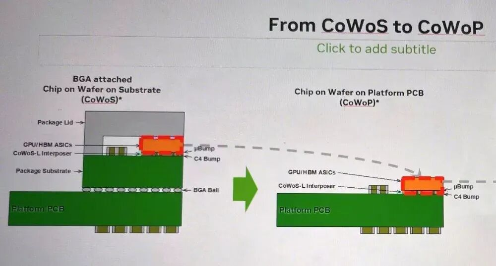
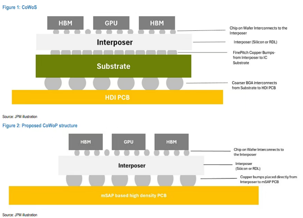
(Schematic of CoWoP Structure: Top to Bottom, compared to CoWoS) CoWoS: GPU/HBM → Interposer → Substrate → PCB CoWoP: GPU/HBM → Interposer → PCB (using mSAP process)
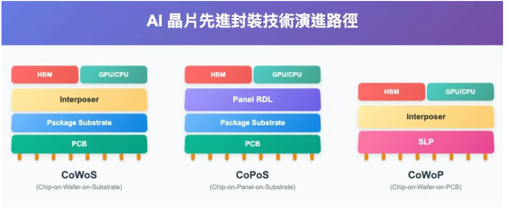
While CoWoP charges forward with its "cost-down" slogan, in TSMC's technology roadmap, CoWoS's true successor might not be CoWoP, but CoPoS (Chip-on-Panel-on-Substrate).
As AI chips grow larger, traditional round wafers face utilization bottlenecks. The core idea of CoPoS is "turning round into square", meaning replacing the round silicon interposer with a rectangular panel-level RDL (Redistribution Layer).
CoPoS's advantage lies in production efficiency. Rectangular panels (e.g., 310x310mm or larger) have far higher area utilization than round wafers, effectively solving production capacity bottlenecks and potentially lowering costs. TSMC has planned to establish a CoPoS pilot line in 2026, aiming for mass production between 2028 and 2029, with NVIDIA reportedly being the first customer.
Comparing the positioning of the three:

The emergence of CoWoP has a polarized impact on the supply chain. For ABF substrate manufacturers, this is undoubtedly bad news, as the value-added of substrates could be significantly reduced. But for PCB manufacturers, this seems like a golden opportunity, as high-end PCBs would directly take on the responsibility of internal package routing.
However, this pie is not easy to eat. Industry insiders bluntly state that CoWoP places extremely high technical demands on the PCB motherboard, mainly facing three major challenges:
Despite the appealing concept, capital markets and foreign institutional investors generally hold a reserved view on CoWoP's short-term prospects.
TF International Securities analyst Ming-Chi Kuo pointed out that Apple took 4 years to complete the ecosystem upgrade when developing its Substrate-Like PCB (SLP). Expecting NVIDIA to introduce CoWoP into mass production for Rubin Ultra within just 1 to 2 years is overly optimistic.
Morgan Stanley and J.P. Morgan also believe that, considering CoWoS's current yield is already close to 100%, forcing a switch to the unproven CoWoP technology in 2026 carries extremely high commercial risk. In contrast, CoPoS, which addresses production efficiency issues, should logically have a higher commercialization priority than CoWoP.
In summary, CoWoS will remain the absolute mainstream in the market for the next five years, and its position is difficult to shake in the short term.
CoWoP is more like a bold probe into the traditional packaging supply chain. It represents the industry's desire to break the substrate monopoly and reduce costs, but limited by technological maturity and the difficulty of supply chain restructuring, it is unlikely to replace CoWoS in the near future.
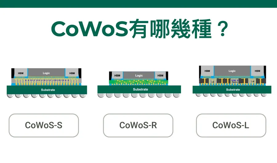
The future battle in advanced packaging will be a three-way game between CoWoS (and its evolved version CoWoS-L), CoPoS (panel-level packaging), and CoWoP (board-level packaging). Regardless of which path prevails, the core logic remains unchanged: In an era of slowing Moore's Law, whoever can provide the strongest interconnection density and thermal performance at the optimal cost will dominate the next decade of AI chips.
