December 18, 2025
HDI (High-Density Interconnect) circuit boards, due to their high-density packaging and multi-layer applications, are widely used but also significantly more expensive than standard PCBs. For Taiwanese PCB designers and product managers, understanding the primary cost drivers and proposing design optimization strategies is crucial. This analysis examines HDI cost structures from three key perspectives: drilling count, lamination layers, and material grades. It also explains how other critical factors can be controlled during the design phase. The article incorporates Taiwan market trends and pricing data for 2024–2025, ensuring both practical relevance and professional accuracy.
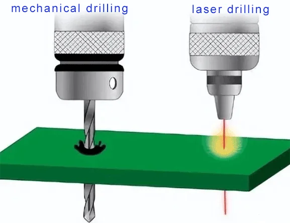
HDI boards have dense via locations, making drilling a major cost component. Traditional mechanical drilling requires expensive drill bits with short lifespans, especially for micro-vias below 0.15mm, which are more labor-intensive. In contrast, laser-drilled micro-blind vias do not require physical drill bits and are relatively low-cost.
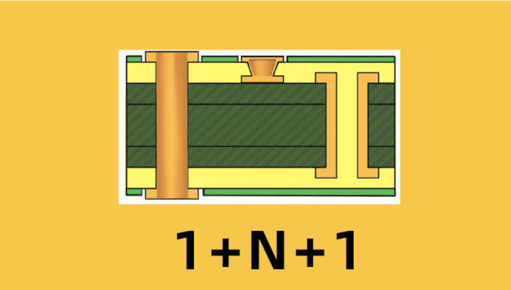
Multilayer HDI boards often require multiple sequential lamination cycles. The more lamination cycles, the higher the cost. Studies show that costs rise with increasing stack-up complexity. Each additional sequential lamination cycle adds a full-board heating and high-pressure process step, along with corresponding multiple drilling and plating steps, equating to substantial additional labor and material costs.
HDI multilayer boards often use mid-to-high-end substrates to enhance thermal stability and mechanical strength, but higher material grades also increase cost.
