Structural Differences and Roles of Blind vs. Buried Vias
Through-Hole Via (Plated Through-Hole, PTH)
- Definition: The most common type of plated hole, penetrating all layers of the PCB to connect top and bottom layers, also providing mechanical support for components.
- Disadvantages: Occupies significant board space and introduces substantial parasitic effects in high-speed signal paths.
Blind Via
- Definition: Drilled from one side (outer layer) of the board to an inner layer without penetrating the entire board, visible only from one outer surface.
- Application: Commonly used for BGA fan-out and high-density routing, allowing signals to connect directly to target inner layers without wasting area on the opposite side.
Buried Via
- Definition: Completely hidden between inner layers, connecting two or more inner copper layers without reaching the outer surfaces.
- Application: Significantly increases interlayer connections without affecting outer layer component layout. Common in boards requiring extensive internal power planes or those with high layer counts.

HDI Board Classification and Structure
HDI boards are typically classified based on the hierarchical structure of blind/buried via usage:
- Type I HDI: Uses a single layer of blind vias (1+N+1 stack-up) with no buried vias.
- Type II HDI: Adds buried vias (e.g., within the core) to the Type I structure, enhancing connection flexibility.
- Type III or Higher-order HDI: Features multiple layers of blind vias, requiring sequential lamination and a combination of blind/buried vias to support ultra-high-density BGA routing.
Summary: Blind vias primarily connect outer layers to adjacent inner layers, while buried vias act as bridges between inner layers, enabling multi-level 3D interconnection.
Aspect Ratio Limitations and Reliability Considerations
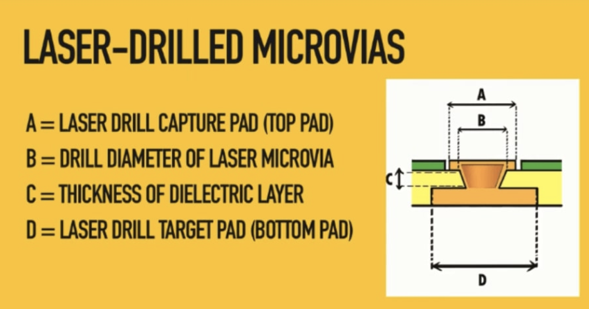
The reliability of blind/buried vias heavily depends on the plating quality of microvias (typically with diameters ≤0.15mm), where the Aspect Ratio (AR)—the ratio of depth to diameter—is a critical parameter.
Technical Standards and Industry Practice
- IPC Standard: The upper limit for microvia aspect ratio is 1:1, meaning the depth should not exceed the diameter, with typical practical depths ≤0.25mm.
- Industry Recommendation: For high reliability, maintain an AR below 0.8:1 during design.
Risks and Consequences
Excessively high aspect ratios (e.g., >1:1) can lead to:
- Thinning of the copper plating on the via wall.
- Difficulty in reworking/repair plating.
- Increased risk of copper cracking or delamination during high-temperature reflow soldering.
IPC 2019 Warning: Microvias with high aspect ratios are prone to failure during reflow cycles.
Design Key Points
- Use the formula: Microvia AR = (Outer Dielectric Thickness + Surface Copper Foil Thickness) / Microvia Diameter for evaluation.
- IPC states the ideal microvia AR is 1:1, while a common design standard is 0.75:1.
- Maintaining a low aspect ratio is key to ensuring complete plating, enhancing mechanical strength, and achieving final reliability.
Impact of Manufacturing Process Sequence on Design
HDI board fabrication involves different process sequences for blind and buried vias.
Process Flow Differences
- Buried Vias: Must be drilled and plated on the inner layer cores before lamination. These sub-assemblies with buried vias are then laminated with other layers.
- Blind Vias: Typically laser-drilled directly from the outer layer after one or more layers are built up. Buried vias within cores may be drilled using laser or mechanical methods depending on diameter.
Lamination Methods
- Boards with Buried Vias: Require Sequential Lamination. Inner layer pairs containing buried vias are first laminated into sub-assemblies, which are then finally laminated with the outer layers.
- Blind Vias: Are usually laser-drilled through the outer dielectric to the target inner layer after building up one or more layers (can also be drilled after partial lamination).
Process Considerations
- Larger diameter holes (like PTHs or some buried vias) often use mechanical drilling, while microvias use UV or CO₂ laser drilling.
- If a design contains both blind and buried vias, the layer hierarchy and drilling sequence must be planned in advance to avoid conflicts between design intent and manufacturing order.
Impact of Via Size on Signal and Electrical Performance
Via size and microvia structure significantly affect Signal Integrity (SI).
Impact of Parasitic Parameters
- Parasitic Capacitance: Primarily from the parallel-plate capacitor effect between the via barrel and adjacent reference planes.
- Influenced by via diameter, spacing to planes, and dielectric constant.
- Larger diameters and narrower spacing increase parasitic capacitance, slowing signal rise times.
- Parasitic Inductance: Primarily proportional to via depth (number of layers or dielectric thickness).
- Via diameter has a minimal effect on inductance.
- Microvias (short and thin) primarily reduce inductance by minimizing depth.
Design Advantages and Recommendations
- Compared to traditional large through-holes, HDI microvias offer shorter propagation paths and lower parasitic loading for high-speed signals due to their smaller size and typical use connecting only adjacent layers, helping reduce reflections and losses.
- In design, minimize excessively long via stubs. On critical high-speed lines, use microvias or back-drilled vias to maintain impedance continuity.
Common HDI Design Pitfalls and Recommendations
Common errors and countermeasures when designing HDI boards include:
1. Unfilled Via-in-Pad
- Problem: If vias placed within component pads are not filled with conductive (copper) or non-conductive (epoxy) material, voids or solder defects are highly likely during reflow.
- Recommendation: Confirm with the manufacturer the use of via fill/cap plating techniques for Via-in-Pad designs to ensure a void-free fill and a planar copper surface.
2. Stacked Via Design
- Problem: Directly stacking microvias on top of each other across layers causes the upper microvia to bear the cumulative thermomechanical stress from the lower ones, easily leading to cracks or pad separation.
- Recommendation: For connections across multiple layers, prioritize staggered vias to distribute stress. Consider stacked vias only where space is extremely critical, the process allows, and after thorough feasibility discussion with the fabricator.
3. Dielectric Thickness and Impedance
- Problem: Ignoring the thickness tolerance of substrate dielectrics during design can lead to significant final impedance deviation.
- Recommendation: Select materials with low dielectric constant (Low-Dk) (e.g., Rogers, Megtron) and agree on strict thickness tolerances with the PCB manufacturer to allow for impedance matching compensation during the design phase.
4. Microvia Spacing and SMD Areas
- Problem: Placing microvias in dense SMD (Surface Mount Device) areas can affect reflow soldering quality, leading to poor solder joints.
- Recommendation:
- Avoid placing microvias in non-pad areas of SMD components.
- If necessary, place them within the pad area and ensure proper filling/capping.
- Maintain adequate spacing (generally ≥0.30mm) between microvias, and between blind/buried vias, to prevent plating issues from one via intruding into another.
5. Layer Registration and Lamination Alignment
- Problem: Ignoring material deformation and drilling misalignment during multi-layer lamination can cause short or open circuits.
- Recommendation: Implementing layer-to-layer alignment compensation in the design tool and performing registration checks during prototyping are essential to ensure high-precision alignment in the actual manufacturing process.
Conclusion
HDI blind and buried via technology is the bridge that transforms millimeter-scale concepts into micron-scale products. Through rational structural planning, strict control of aspect ratio and via size, and a deep understanding of the manufacturing sequence, designers can balance signal integrity with manufacturing reliability in high-density layouts.
As industry experts note, traditional through-holes can no longer meet the demands of advanced applications. The "invisible channels" of HDI are key to achieving small form factors and high connection density. Proficient designers must master the principles and considerations outlined above to successfully achieve the design goals of high-density interconnect boards while balancing performance, reliability, and cost.
