December 20, 2025
Many people encounter a common pain point during prototyping: the signal eye diagram looks perfect in simulations, but when the board arrives for testing, severe signal attenuation or impedance mismatch occurs. The devil often lies in the details the datasheet doesn't mention—fluctuations in dielectric constant (Dk), the true behavior of the loss tangent (Df), and symmetry traps within HDI stackups.
This article will reveal these hidden variables to help you precisely avoid pitfalls during PCB prototyping.
Many engineers are accustomed to entering a fixed Dk value (e.g., 4.2 for FR-4) in tools like Polar Si9000. However, in the world of high frequencies, Dk is not a constant.
Even for laminates of the same grade/model, the Dk can differ significantly based on the Glass Style. This is due to the differing mix ratio between glass fabric (Dk~6.0) and resin (Dk~3.0).
| Glass Style | Resin Content (RC%) | Dk @ 10GHz (Megtron 7) | Application Suggestion | | :--- | :--- | :--- | :--- | | 1027 / 106 | High (~75%) | 3.15 | HDI buildup layers, easier for laser drilling | | 1078 / 1080 | Medium (~63%) | 3.35 | General signal layers | | 7628 | Low (~45%) | 3.60 | Core layers, high mechanical strength |
Practical Advice: In high-frequency HDI design, never mix different types of Prepreg (PP) within the same impedance-controlled layer. This will cause inconsistent propagation delay along a trace, resulting in severe Skew (timing skew).

Above 10GHz, Dielectric Loss becomes the key factor determining how far a signal can travel. We've compiled key data for three mainstream high-frequency materials for your reference:
| Material Vendor | Product Series | Dk @ 10GHz | Df @ 10GHz | Loss Characteristics | Typical Application | | :--- | :--- | :--- | :--- | :--- | :--- | | Panasonic | Megtron 6 | 3.61 | 0.004 | Ultra-Low Loss | Servers, Networking | | Rogers | RO4350B | 3.48 | 0.0037 | Ceramic / RF | 5G PA, Antennas | | Isola | Tachyon 100G | 3.02 | 0.0021 | Extreme Low Loss | 100G Backplanes |
Even if you select a top-tier material like Tachyon 100G, pairing it with standard foil (STD Copper) will still cause signal attenuation. This happens because the "Skin Effect" forces current to travel a longer, more lossy path on the rough surface.
In a standard 8-layer HDI (2+N+2) design, L3 and L6 are typically designated as high-speed Stripline layers. Sandwiched between two ground planes (GND), they offer the best EMI shielding.
A traditional Through Hole connecting L1 to L3 leaves a dead-end section from L3 to L8, creating an antenna-like Stub. For 25Gbps signals, a stub longer than 10mil can create a fatal resonant notch. The advantage of HDI lies in using Blind Vias and Buried Vias to precisely connect L1-L2-L3, completely eliminating the Stub effect. This is the fundamental physical reason why high-speed designs must adopt HDI.
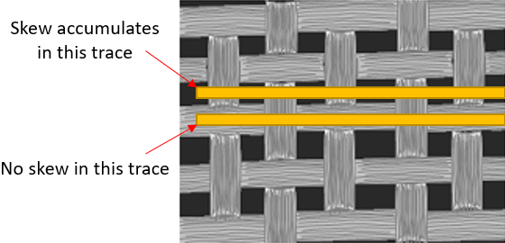
This is a commonly overlooked "phantom" issue. The glass fabric in PCBs is woven from warp and weft threads, creating "Bundles" and "Gaps."
In high-frequency PCB design, impedance control is a precise game of material science. To ensure your design yields high-quality prototypes with Taiwanese PCB manufacturers, pay attention to the following points when outputting Gerbers and specifying requirements:
Taiwan possesses the world's most complete PCB supply chain. Choosing a prototyping partner who understands the technology and can provide DFM (Design for Manufacturability) advice is key to your product's success from R&D to mass production. We hope this guide serves as a strong support for your R&D journey, helping your signals travel faster, more stably, and farther.
