December 24, 2025
This report will provide an in-depth analysis of the most critical process in PCB manufacturing—inner layer fabrication—spanning over 15,000 words.
In Taiwan, a technological fortress often called the "Silicon Island," the brilliance of the semiconductor industry often overshadows another equally critical field—Printed Circuit Boards (PCBs). If chips (ICs) are the brains of electronic products, then PCBs are undoubtedly the skeleton connecting nerves and blood vessels. For many Taiwanese electrical engineering students, novice layout engineers, and even seasoned hardware R&D personnel, PCBs are often a familiar yet mysterious "black box." We draw beautiful schematics on computers using EDA software, send out Gerber files, and receive a green board a few weeks later. But what exactly happens in between? Why do factory technicians often say traces are "washed" out? Why is an inner layer board "unsalvageable" once it's ruined?
We will delve into the physical and chemical principles of its core philosophy, the "Subtractive Process," and analyze key variables affecting yield from multiple dimensions including material science, fluid dynamics, and optical inspection.
More importantly, under the wave of "Industry 4.0" and "Digital Twin," the traditional "Trial and Error" manufacturing model has reached its limits. As trace width/spacing approaches physical limits, simulation and prediction at the design stage have become unprecedentedly important. This is precisely the critical moment for advanced EDA cloud platforms like eCloud to intervene. By shifting manufacturing parameters to the design stage for simulation, we can not only predict electrical performance but also foresee process risks, avoiding "dead boards" from the source.
In an era where "Additive Manufacturing" like 3D printing is increasingly popular, mainstream PCB processes still firmly hold the ground of the "Subtractive Process." The so-called "washing," in Taiwanese factory terminology, refers to Etching.
Imagine a complete copper sheet. Like a sculptor, we use chemical agents to corrode ("wash") away the unwanted copper, leaving behind the conductive traces we need. This process sounds simple, but at the micron (µm) scale, it involves extremely complex chemical kinetics and fluid control. Any minor deviation in any link—whether uneven exposure energy, fluctuating development pressure, or drifting etch chemical concentration—can lead to trace deformation, breakage, or short circuits.
This report is written for Taiwanese electronic engineers, PCB practitioners, and students in related fields. We will use industry-standard Taiwanese terminology (e.g., "Cut Lamination," "Lamination," "Short-Open Test") combined with academic theory, aiming to establish a complete knowledge system from Design to Manufacturing.
Through this report, readers will be able to:
The starting point of all processes begins with an insulating sheet covered with copper foil—Copper Clad Laminate (CCL). For designers, this might be just a parameter in software settings (e.g., FR4, Dielectric Constant), but for process engineers, it's the physical foundation determining all subsequent process windows.
CCL primarily consists of three parts. The interaction of these three determines the board's electrical, thermal, and mechanical properties.
For inner layer processes, we typically use Electrodeposited Copper Foil.
Resin is the matrix of the substrate, most commonly Epoxy.
Fiberglass Cloth provides mechanical strength to the substrate.

Cutting is not merely slicing large-sized base material (Sheet) into the work size required by the production line (Panel, e.g., 18"x24"). It is more importantly a process of stress management.
Dust is the major enemy at the cutting stage. If fiberglass dust adheres to the copper surface, it becomes an obstacle point for subsequent exposure/development, causing "pinholes" or shorts on traces. Therefore, modern cutting machines are equipped with powerful automatic dust collection and static elimination devices.
After cutting, panels are usually sent into an oven for prolonged baking (e.g., 150°C for 4-8 hours).
The application value of the eCloud platform at this stage lies in its ability to simulate the deformation of different cutting sizes and panelization layouts under heat based on the Coefficient of Thermal Expansion (CTE) data provided by laminate suppliers. This assists factories in optimizing material utilization while predicting and compensating for expansion/contraction.
| Parameter | Impact Area | Risk with Traditional Approach | eCloud Solution | | :--- | :--- | :--- | :--- | | Warp/Weft Direction | Expansion Rate, Warpage/Twist | Prone to material mix-up leading to warpage | Digitally mark material direction, simulate stack-up symmetry | | Copper Foil Roughness | Signal Integrity, Adhesion | Sacrificing SI performance for yield | Simulate impact of different roughness on SI, seek optimal balance | | Moisture Content | Popcorning Risk | Relying solely on experience to set bake time | Establish material moisture absorption model, optimize baking parameters |
The key to transforming a copper sheet into a circuit board lies in precisely "printing" the design pattern onto the copper surface. This involves the precise collaboration of surface chemistry and photochemistry.
The copper foil surface oxidizes rapidly upon contact with air and may be contaminated with grease. If photosensitive Dry Film is laminated directly, adhesion will be poor, leading to chemical seepage under the resist during subsequent etching, causing jagged trace edges or even breaks.
The pre-treatment line typically includes acid cleaning, degreasing, micro-etching, rinsing, and drying.
In a cleanroom (typically a yellow light area to prevent UV from pre-exposing the dry film), a laminator is used to apply the dry film onto the treated panel surface.
Dry film is not a single layer; it's like a sandwich:
Lamination quality depends on the synergy of three parameters:
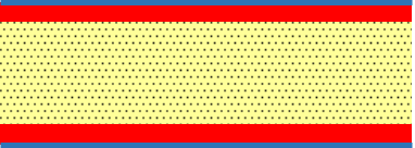 (Cross-section after coating)
This is the soul of pattern transfer. We use Ultraviolet (UV) light to irradiate the dry film.
The inner layer process overwhelmingly uses negative photoresist.
Traditional exposure uses a Phototool/Film, which expands/contracts with temperature/humidity and is easily scratched, a fatal flaw for large panels or High-Density Interconnect (HDI) boards.
LDI (Laser Direct Imaging) technology directly receives digital data from the CAM station and uses a laser beam to scan and image the panel surface.
These three steps are usually performed continuously in an in-line horizontal wet process line (DES Line: Developing, Etching, Stripping). This is the battleground of the "Subtractive Process" and a high-risk area for yield loss.
Uses a weakly alkaline solution (typically 1% sodium carbonate Na₂CO₃, at about 30°C) to wash away the unpolymerized (unexposed) dry film.
Developing is not about washing longer the better. Polymerized dry film can also slowly swell or soften in alkali.
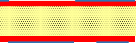 (Cross-section after development)
This is the process of dissolving away the exposed copper (originally the unexposed areas).
Inner layer etching commonly uses acidic Cupric Chloride (CuCl₂) etchants.
Metallic copper is oxidized by cupric ions (Cu²⁺) into cuprous chloride (CuCl, insoluble in water). To sustain the reaction, Hydrochloric acid (HCl) and an oxidizer (like hydrogen peroxide H₂O₂) must be added to rapidly regenerate cuprous back into cupric ions.
This is a dynamic equilibrium system. An auto-dosing system monitors the solution status using a colorimeter or Oxidation-Reduction Potential (ORP) meter, precisely controlling the addition of HCl and H₂O₂.
This is physics playing a trick on engineers. When etchants spray onto the panel surface, they corrode not only downwards (vertical direction) but also sideways (horizontal direction), digging under the protective dry film resist. This is called Undercut.
A higher etch factor means less undercut and squarer traces, which is more favorable for Impedance Control. Traditional processes have an etch factor of about 3-4, while high-end processes pursue 6 or above.
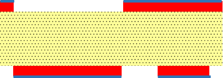 (Cross-section after etching)
The Key Role of eCloud: At the design stage, engineers often assume traces are rectangular. But the actual trapezoidal shape from manufacturing leads to higher impedance. eCloud's advanced simulation engine can import the factory's actual etch factor data, reconstruct a true conductor cross-section model, and perform more accurate field solver calculations. This guides engineers to adjust trace widths at the layout stage to counteract impedance deviation caused by etching.
After etching is complete, the dry film that protected the traces has served its purpose. A strong alkali (2-5% NaOH or KOH, at about 50-60°C) is used to strip away the polymerized dry film. After stripping, cleaning, and drying, the panel reveals the inner layer traces we see.
 (Cross-section after stripping)
After inner layer fabrication is complete, it must undergo strict inspection. Because once it proceeds to the next step—Lamination—the inner layer is permanently sealed with no way back.
The human eye cannot inspect thousands of hair-thin traces (e.g., 3 mil = 75 µm). AOI (Automated Optical Inspection) uses high-resolution CCD cameras to scan the panel surface, capturing images based on the optical contrast between the copper surface (strong reflection) and the substrate (weak reflection).
Defects detected by AOI are an important data source for process improvement.
| Defect Name | Phenomenon Description | Possible Root Cause | | :--- | :--- | :--- | | Open | Trace break | Dry film scratched before exposure; overdevelopment; overetching; panel surface contaminated causing resist peeling. | | Short | Two traces connected where they shouldn't be | Excessive exposure energy (diffraction); unclean development (scum); insufficient etching; residual adhesive on dry film. | | Nick | Notch/indentation on trace edge | Dirt/particle on exposure film; poor dry film adhesion (seepage). | | Pin Hole | Small holes on traces | Air bubbles trapped during lamination; impurities mixed into dry film. |
AOI is not omnipotent. If the panel surface has uneven oxidation color, or the substrate weave texture is too deep, AOI might misjudge it as a defect (False Call), requiring manual Verification/Repair Station (VRS) and consuming significant manpower. More可怕的是漏报 (Escape), where real defects are not caught and flow to subsequent processes, causing final product failure. This is why high-end AOI equipment is beginning to incorporate AI deep learning technology to reduce misjudgment rates.
This is the biggest question for many beginners: "Why can't we just replace the bad part like repairing a motherboard?" To answer this, one must understand the upcoming Lamination process.
PCB lamination involves stacking multiple inner layer cores with Prepreg (PP) sheets together and bonding them into one under vacuum, high temperature, and high pressure.
Once lamination is complete, inner layer traces are sandwiched between hard glass-fiber resin composite materials.
Therefore, inner layer Scrap is absolute. For a 20-layer high-end server board, if a microscopic open on layer 3 goes undetected and is only found during final testing after lamination, then all material costs, processing fees for the preceding layers, and the costs of subsequent outer layer processes (drilling, plating, solder mask) are all wasted. This is why PCB factories are近乎偏執 about controlling inner layer yield.
Having understood the limits and risks of traditional processes, we can appreciate why Electronic Design Automation (EDA) cloud platforms (like eCloud) are becoming the new standard for the industry. This is not just a tool upgrade but a paradigm shift in design thinking.
Traditionally, Layout engineers only drew schematics, rarely considering "manufacturability" or "laminatability." This led to many designs requiring significant modifications at the factory (CAM) stage (e.g., adding teardrops, adjusting trace widths) or even being unmanufacturable.
The eCloud platform integrates parameters and knowledge from the manufacturing side:
For students and freelance engineers, using a platform like eCloud means your design is Manufacturable. What you deliver is not just a Gerber file, but a verified production plan. This can significantly reduce time spent on back-and-forth communication with factories (Engineering Queries, EQ), shortening Time-to-Market. In Taiwan's industry environment that emphasizes speed and quality, this is your core competitiveness and credibility.
From a copper clad laminate to , we have witnessed a spectacular dance of optics, chemistry, fluid dynamics, and material science. Each step—from stress relief during cutting, microscopic adhesion of dry film, precise alignment in exposure, to the dynamic balance of etching—challenges the limits of physics.
Although the "Subtractive Process" seems like simply "washing" away the excess, it is actually a war against tolerances. In this process, any minor can be permanently magnified after lamination, becoming an irrecoverable loss. This also explains why the PCB industry's pursuit of yield and reliability is endless.
However, with the advancement of Moore's Law, relying solely on veteran experience and post-inspection is no longer sufficient to meet future challenges. Digital Twins and cloud simulation (like eCloud) are reshaping this industry. They move the "trial and error" process from expensive factory production lines to a zero-cost virtual space, allowing designers to foresee the future and manufacturers to grasp the variables.
For Taiwan's young engineers and students, deeply understanding these process details and skillfully using advanced digital tools will be the key step in your progression from "draftsman" to "architect." In this era where electronic products are ubiquitous, mastering the secrets of PCBs is equivalent to mastering the skeleton of the technological world.
| Traditional Chinese Term | English Term | Industry Usage / Explanation | | :--- | :--- | :--- | | 開料 | Cut Lamination | Cutting base material into work size (Panel Size) | | 內層 | Inner Layer | Conductive layers inside a multilayer board | | 減除法 | Subtractive Process | Process of using etching to remove unwanted copper | | 銅箔基板 | CCL (Copper Clad Laminate) | Raw material for PCB | | 乾膜 | Dry Film Photoresist | Photosensitive resist for pattern transfer | | 曝光 | Exposure | Using UV light to polymerize/harden dry film | | 顯影 | Developing | Using weak alkali to wash away unexposed dry film | | 蝕刻 | Etching | Using acid to corrode away unwanted copper | | 側蝕 | Undercut | Sideways etching under resist, causing trapezoidal traces | | 去膜 | Stripping | Using strong alkali to remove protective dry film | | 壓合 | Lamination | Bonding inner layers and PP sheets under high temp/pressure | | 半固化片 | Prepreg (PP) | Resin-impregnated fiberglass sheet for bonding layers | | AOI | Automated Optical Inspection | Machine for automated optical inspection | | DFM | Design for Manufacturing | Designing for ease of manufacturing | | 阻抗控制 | Impedance Control | Controlling trace characteristics to ensure signal integrity | | 死板/報廢 | Scrap | Non-repairable defective product |
