December 24, 2025
Continuing from the previous discussion on inner layer etching, we now have several inner layer core boards with their traces “washed” clean. However, these are not yet the PCBs we are familiar with; at best, they are merely stacks of thin copper foil and fiberglass.
Next, we enter what seems like the "black magic" stage of PCB manufacturing—Lamination. Why "black magic"? Because we take several boards, stack them together, send them into a high-temperature, high-pressure furnace, and they emerge as a single, solid block. Moreover, the 10 or 20 layers of circuitry buried inside must be perfectly aligned, with tolerances less than half the diameter of a human hair.
This stage is critical for the success or failure of a multi-layer board. Today, we will thoroughly dissect the complete process from Brown Oxide treatment, lay-up, lamination, X-ray drilling, to mechanical drilling, and answer a question that plagues countless engineers: Why do the hole positions shift from my perfectly aligned CAD design to the finished board from the factory?
Before stacking the inner layers, there is an absolutely essential surface treatment step. The early process was called "Black Oxide," but today, mainstream high-end processes in Taiwan predominantly use Brown Oxide.
The copper surface of an inner layer after etching is smooth metal. If you were to directly bond it with prepreg (PP, or bonding sheet), it would be like using adhesive tape on glass—it might stick initially, but it's prone to delamination under heat or stress (e.g., during reflow), commonly known as "blistering" or "popcorning."
The purpose of brown oxide treatment is to use a chemical solution to "grow" a layer of organic-metallic fuzz on the copper surface.
The early black oxide layer featured an acicular (needle-like) crystal structure. While it provided excellent adhesion, it was prone to the Pink Ring phenomenon—during subsequent drilling, acidic solutions could attack the oxide layer from the side, dissolving the copper oxide and revealing the pink base copper underneath. The brown oxide layer has a granular or nodular structure with better acid resistance, significantly mitigating the pink ring issue.
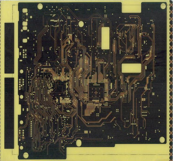
| Characteristic | Black Oxide | Brown Oxide | | :--- | :--- | :--- | | Structure | Acicular (Needle-like) Crystals | Granular/Nodular Structure | | Adhesion | Excellent | Very Good | | Acid Resistance | Poor, prone to Pink Ring | Good, mitigates Pink Ring | | Application | Early processes, lower-end boards | Modern mainstream high-end processes |
This step involves stacking the inner layer cores and PP sheets in sequence, preparing them for the laminating press. It requires a high-cleanliness environment, typically performed in a cleanroom, to prevent dust from causing inter-layer shorts or high-voltage breakdown.
PP is the "glue" of the PCB and the insulating dielectric between layers. It's made of fiberglass cloth impregnated with epoxy resin and is in a B-Stage (semi-cured state).
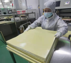
The stacked boards are sent into a vacuum hot press, where engineers must meticulously design the Press Cycle. It's not just about heating; it's a race against viscosity:
At the design stage, we often assume the post-lamination dielectric thickness is fixed (e.g., 4 mils). However, the actual Copper Area (residual copper ratio) affects the thickness. If one layer has very little copper (sparse), resin will heavily fill the areas where copper was etched away, causing the final thickness in that region to become thinner.
This is the most troublesome physical phenomenon in lamination and the root cause of misalignment in multi-layer boards.
When the board material is laminated at high temperatures (~180°C), it expands. However, after the resin cures and locks the structure, different materials contract at different rates as they cool back to room temperature:
This mismatch in Coefficient of Thermal Expansion (CTE) causes inner layers to typically shrink after lamination. Moreover, fiberglass cloth has a Warp (length) and Weft (width) direction, each with a different shrinkage rate!
A 24-inch board might shrink by 0.05% to 0.1% after lamination. That sounds small? 24 inch * 0.1% = 24 mils = 0.6 mm. For a via with a diameter of only 0.2 mm, a 0.6 mm shift means the drill could miss the target pad entirely, causing breakout or an open circuit.
The factory's CAM engineers don't produce using your 1:1 Gerber data. They pre-scale the inner layer films based on an empirical database (big data).
After lamination, the inner layer target pads are completely covered by the outer layer copper foil, invisible to the naked eye. How do we know where the inner layer traces actually are and how much they've shrunk?
This is where the ultimate tool comes in: the X-ray Drilling Machine.
For high-end HDI boards or large boards over 20 layers, simple linear scaling (uniform scaling of the entire board) is no longer accurate enough. This is because the shrinkage rate at the board's center and edges may differ. Advanced X-ray machines employ Zone Scaling, dividing the board into several zones and applying different scaling factors to each. This is the ultimate method for solving layer shift in high-end boards.
With the tooling holes in place, we proceed to the CNC drilling machine. The challenge here is: How to drill through copper and fiberglass at tens of thousands of RPM without the drill bit wandering?
You'll notice that PCB drill bits typically have a 130° point angle, unlike the 118° common in metalworking.
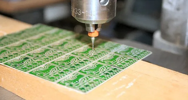
For efficiency, factories typically drill 2-3 boards stacked together.
After reading this, you might think: "Scaling and compensation are the factory CAM's job. What does it have to do with my layout design?"
That's a big misconception! Design sets the ceiling for yield. Factory compensation techniques can only recover so much. If your design is inherently flawed, even the best process can't fix it.
Copper Balance Analysis: Uneven copper distribution is a primary cause of uneven scaling. If your PCB has a dense copper pour on the left and only a few traces on the right, the stress after lamination will differ, causing the board to warp or twist.
Stackup Symmetry Check: eCloud checks if your layer stackup is symmetrical (e.g., whether the copper weight on Layer 2 equals that on Layer n-1). An asymmetrical stackup is the biggest culprit behind post-lamination bow and twist.
Manufacturable Annular Ring Check: Considering factory drilling tolerances (+/- 3 mils) and scaling errors, are your via pads large enough?
Material Library Simulation: eCloud is linked to real material databases (like those from Taiwan vendors). You can select specific PP types in the software, and the system will predict the actual post-lamination dielectric thickness based on their flow characteristics, moving your impedance calculations from "paper theory" towards reality.
Lamination is the critical moment when a PCB transitions from a 2D plane to a 3D structure, and drilling is the precise surgery connecting its neural layers. "Layer shift" and "dimensional stability" are inherent physical properties of materials that cannot be eliminated, only managed through prediction and compensation.
For Taiwanese engineers pursuing high quality, leveraging eCloud for proactive DFM checks and precise stackup simulation allows you to circumvent these manufacturing risks from the very source. After all, it's far better to solve problems with digital tools during the design phase than to sigh over a pile of scrapped boards during prototyping!
Next, we will enter the PCB's "vascular" reconstruction phase—desmear and plating, exploring how to make non-conductive hole walls conductive with copper!
