1. Introduction: Breaking the "What You See Is What You Get" Digital Illusion
In the modern electronic hardware development workflow, Layout Engineers and R&D often spend weeks or even months designing schematics and routing PCBs in EDA tools (such as Altium Designer, Cadence Allegro, or Mentor Graphics). On the high-resolution screens of a computer, a Via is a perfect cylinder, a Trace is a rectangular copper foil with sharp edges, and layer-to-layer alignment is a mathematical coordinate overlap with absolute precision. This "What You See Is What You Get" (WYSIWYG) digital illusion often leads designers to mistakenly believe that PCB manufacturing is as simple as printing an image on paper with an inkjet printer.
However, from the moment the Gerber files are transmitted to the Fab House, these idealized digital data points must undergo a harsh physicochemical transformation. PCB manufacturing is not simple graphic replication; it is a series of processes that challenge material physical limits on a microscopic scale. From the intense thermal stress caused by mechanical drilling on Epoxy and Fiberglass composites, to the atomic-level Nucleation of electroless copper on non-conductive surfaces, to the diffraction and penumbra effects of UV light on Dry Film during lithography—every step hides "invisible killers" that can lead to final product failure.
For products pursuing High Reliability and Signal Integrity (SI), understanding these process details is no longer the sole responsibility of the board house; it is an essential literacy for the design side. A minor design oversight, such as an excessive Aspect Ratio or an overly tight Annular Ring, can trigger catastrophic Low Yield in mass production or even cause Field Failures in the hands of the end customer.
This article focuses on the three core steps of converting an insulating Laminate into a precision interconnection carrier—PTH, Plating, and Exposure—revealing the deep mechanisms rarely mentioned in datasheets but which directly determine PCB reliability and electrical performance.
2. Pre-processing: Drilling & Desmear — Repairing Physical Damage
Before entering the chemical copper process, we must first discuss Drilling and the subsequent Desmear process, as these form the physical foundation determining via quality.
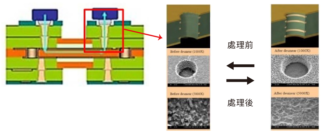
2.1 Drilling Heat & Smear Formation
Mechanical drilling is a high-speed (typically 150k - 300k RPM) and high-feed cutting process. As the Drill Bit penetrates copper foil, fiberglass, and resin, it generates immense frictional heat.
- Resin Melting: When the instantaneous temperature in the drilling zone exceeds the resin's Glass Transition Temperature (Tg, typically 130°C - 170°C for FR-4) or even its melting point, the resin transitions from a glassy state to a rubbery or fluid state.
- Smear Smearing: The Flute of the drill bit is responsible for chip removal, but the melted resin can easily be dragged by the bit and smeared onto the cross-section of the newly cut Inner Layer Copper Ring. This insulating resin film is called "Smear."
- Consequences: If this smear is not thoroughly removed, the subsequent chemical copper will deposit on the smear rather than directly contacting the inner layer copper ring. This forms an electrical "False Connection." During high-temperature Reflow or thermal shock testing, the resin expands, causing the smear to fracture, leading to Interconnect Defects (ICD) or Opens.
2.2 The Chemical Mechanism of Desmear
To remove smear and ensure electrical connection, the industry standard is the Permanganate process. This is not just cleaning; it is a restructuring of the hole wall.
- Swelling: An alkaline solvent (like glycol ethers) penetrates the resin structure on the hole wall surface, softening and swelling it to break the Van der Waals forces between polymer chains, preparing for the oxidation reaction.
- Permanganate Etch: This is the core step. In a high-temperature (approx. 70-80°C) alkaline environment, permanganate ions act as strong oxidants, attacking the carbon-carbon and carbon-hydrogen bonds in the resin molecules.

*Critical Function:* This reaction not only removes the smear covering the copper ring but also etches countless micron-level honeycomb-like **Microporous structures** on the resin surface of the hole wall. These micropores provide crucial **"Anchor Points"** for the subsequent PTH process, drastically improving the mechanical bonding force between the chemical copper and the resin substrate.
3. Neutralization: An acidic reducing agent (like sulfuric acid mixed with hydrogen peroxide or oxalic acid) reduces the residual heptavalent and hexavalent manganese to soluble divalent manganese, thoroughly cleaning the hole wall.
 (Cross-section after Drilling)
eCloud DFM Warning:
- Material Selection: High Tg materials (Tg > 170°C) have stronger chemical resistance and thermal stability. This means they are harder to melt during drilling (less smear) but also harder to etch with permanganate to achieve sufficient roughness. Therefore, for High Tg boards, the Fab House must adjust desmear parameters or switch to Plasma desmear.
- Over-Etch: Excessive etching leads to "Resin Recession," where the hole wall resin retracts behind the glass fiber bundles, creating an uneven hole wall that traps liquid and causes Delamination (explosive board failure).
3. Step One: PTH (Electroless Copper) — The Microscopic Magic of "Creating Something from Nothing"
After desmear, the PCB is still an insulator. To establish a conductive layer on insulating resin and fiberglass, we must rely on Electroless Plating, also known as PTH (Plated Through Hole).
3.1 Palladium Activation: The Fuse for Chemical Deposition
Copper ions cannot spontaneously reduce on a plastic surface. We need a catalyst.
- Sensitization & Activation: Traditional processes use a colloidal solution of stannous chloride and palladium chloride. Tin ions wrap around palladium atoms to form a protective layer. When the board is dipped into the activation bath, colloidal palladium adsorbs onto the negatively charged hole wall surface.
- Acceleration: An acidic solution removes the outer tin shell, exposing the catalytically active metallic Palladium (Pd) core. These palladium cores act as the "seeds" for subsequent copper atom growth.
3.2 Chemical Copper Reaction Mechanism: Autocatalytic Chain Reaction
Entering the chemical copper bath, a precise redox reaction occurs. A system using Formaldehyde (HCHO) as the reducing agent is most common. The reaction must occur in a strongly alkaline environment (pH > 12).
The overall reaction is:

This is an Autocatalytic reaction:
- Initiation: Copper ions in the solution gain electrons on the surface of the "Palladium seeds" on the hole wall, reducing to metallic copper.
- Growth: Once the first layer of copper atoms is deposited, the copper itself also possesses the ability to catalyze the oxidation of formaldehyde. Therefore, the reaction can continue on the newly generated copper layer, allowing it to gradually thicken.
- Thickness Control: Typical chemical copper thickness is only 0.5 ~ 1 µm. This layer is extremely thin, acting only as a conductive seed layer, and cannot withstand high current.
3.3 Engineer's Pain Points: Deep Analysis of Failure Mechanisms
3.3.1 Hole Wall Separation (Pull Away) & Inner Layer Breakage
This is the biggest headache in reliability testing. Cross-sections show the hole copper separating from the substrate, or a black fracture line between the inner layer copper foil and the hole copper.
- Root Cause: Incomplete desmear. If a trace amount of transparent resin film remains on the inner layer copper ring, the chemical copper will grow on top of it but fail to form a true Metallurgical Bond.
- Thermal Stress Mechanism: The Z-axis Coefficient of Thermal Expansion (CTE) of FR-4 substrate (approx. 50-70 ppm/°C pre-Tg; 250-300 ppm/°C post-Tg) is far greater than that of copper (approx. 17 ppm/°C). During Reflow (260°C), the substrate expands dramatically, "pulling" the hole copper away from the inner layer copper ring. If smear exists, this interface is the weakest link and will snap immediately.
3.3.2 Wicking Effect & CAF Risk
- Phenomenon: Under a microscope, hole wall copper appears to seep into the gaps of the glass fiber bundles like tree roots. Depth is usually controlled within 80-100 µm (depending on IPC standards).
- Cause: Mechanical stress during drilling shatters the interface between the fiberglass and resin, or a blunt drill bit pulls at the fiberglass. During desmear and PTH, chemicals use capillary action to penetrate these micro-cracks.
- CAF (Conductive Anodic Filament) Threat: Wicking shortens the insulation distance between conductors. In environments with humidity and Bias Voltage, copper ions can migrate along the glass fiber bundles, growing conductive filaments that lead to insulation failure or board burning.
3.3.3 Aspect Ratio Limitations on Fluid Dynamics
- Definition: The ratio of board thickness to hole diameter (e.g., 3.0mm thickness / 0.3mm diameter = AR 10:1).
- Mass Transport Limitation: The chemical copper reaction consumes HCHO and produces hydrogen bubbles. Inside deep holes, it is difficult for fresh chemicals to enter and for reaction products (hydrogen gas) to exit.
- Result: The reaction rate at the center of the hole is far lower than at the opening, resulting in an extremely thin or even discontinuous copper layer at the center. This is the most common cause of scrap in high aspect ratio boards (like Backplanes).
3.4 eCloud DFM Advice for Layout/RD (PTH Section)
- Strictly Control Aspect Ratio:
- AR < 8:1 is the safe zone for standard processes.
- 8:1 ~ 10:1 requires the Fab House to have better process capabilities.
- > 10:1 enters the high-risk zone, typically requiring special Pulse Plating or vertical continuous plating equipment, significantly increasing costs.
- Avoid Extreme Small Holes in Thick Boards: While laser drilling (Microvia) can achieve 0.1mm, that is for blind vias. For through-holes, try to keep them above 0.25mm (10mil). Larger diameters favor fluid exchange, effectively reducing the risk of voiding (no copper) in the hole.
- Watch Material Tg & Fillers: For high-layer-count boards, choose High-Tg materials. If using filler-containing boards (e.g., ceramics for heat dissipation or CTE control), note that drill bits wear extremely fast, exacerbating Wicking effects. Remind the Fab House to shorten the Drill Hit Count setting.
4. Step Two: Panel Plating — The Physics Game of Current Distribution
The chemical copper layer (~0.5 µm) is too thin and fragile to withstand the erosion of developing solution during subsequent pattern transfer, nor can it carry current. Therefore, Electrolytic Plating is required to thicken the copper to 5-8 µm (as base copper for pattern plating) or to full thickness.
4.1 Electrochemical Principles & The "Dog-bone" Effect
This is the most counter-intuitive physical phenomenon in plating. Layout Engineers often set "Via Copper Thickness 25 µm" and assume it is uniform. In reality, current distribution on geometric surfaces is extremely uneven.
- Faraday's Law & Field Lines: Metal deposition is proportional to the amount of charge passed. Electric Field Lines tend to concentrate at the sharp points and edges of conductors (Edge Effect).
- Hole Opening vs. Hole Center: At the corner (Knee) of the through-hole, field lines are most dense, Current Density (i) is highest, and copper ions deposit fastest. Conversely, the interior of the hole is shielded by the copper layers on the top and bottom surfaces; field lines struggle to penetrate, leading to low current density and slow deposition.
- Dog-bone: This uneven deposition results in extremely thick copper at the hole opening (potentially narrowing or blocking the hole), while the copper thickness at the center barely meets standards. In cross-section, the copper layer looks like a bone—large at both ends, thin in the middle.
4.2 The Additive War: Brighteners vs. Levelers
To combat these laws of physics, modern plating baths use complex organic additive systems—a war at the molecular level:
- Accelerator/Brightener: Small sulfur-containing molecules (like SPS). They adsorb onto the copper surface, lowering the activation energy for reduction and accelerating copper growth.
- Suppressor/Carrier: Long-chain polymers (like PEG). They work synergistically with chloride ions in the solution to form a dense barrier film on the cathode surface, increasing polarization resistance and inhibiting copper growth.
- Leveler: This is the key to solving the Dog-bone effect. Levelers are usually positively charged (like quaternary ammonium salts) and are easily attracted to areas with strong negative charge and high current density (i.e., hole openings and tips).
- Mechanism: Levelers prioritize "occupying" the hole opening positions, strongly inhibiting the copper deposition rate there. Meanwhile, inside the hole where leveler concentration is low (slow diffusion), the Accelerator dominates, allowing copper to grow faster than at the opening.
- Result: This "suppress the strong, support the weak" mechanism allows the internal copper thickness to catch up to the opening, drastically improving Throwing Power (TP). Higher TP values mean the internal/external copper ratio is closer to 1:1.
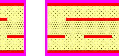 (Cross-section after Plating)
4.3 eCloud DFM Advice for Layout/RD (Plating Section)
- Isolated vs. Dense Holes:
- Phenomenon: In a large area of ground copper, a single Isolated Via will attract all surrounding field lines, resulting in extremely high current density for that hole.
- Risk: The hole may experience "Burning" (rough, blackened copper) or the opening may be plated too thick, shrinking the diameter and causing insertion issues for DIP components.
- Countermeasure: Fab Houses often add "Thieving Pads" (or Dummy Pads) around isolated holes during the CAM stage to disperse current. Layout Engineers should understand and allow this modification, or maintain relatively uniform hole distribution during design.
- Copper Balance:
- If one side of the PCB is a large copper plane (high current consumption) and the other is fine traces (low current consumption), it causes uneven current distribution across the panel.
- Action: Always use the Copper Pour function in EDA software to place grid or solid copper (Dummy Copper) in empty areas. This is not just to reduce etchant consumption (environmental); it is crucial for plating uniformity to ensure consistent copper thickness across the board.
- Understanding Hole Size Tolerances & Plating Compensation:
- When you specify 0.3mm ±0.075mm, the factory will choose a 0.35mm or 0.4mm drill bit. This is to reserve room for 20-25 µm of copper thickness on the walls.
- Misconception: Do not assume the drilled size is the final size. For Non-Press-fit holes, try to relax tolerances to give the factory a larger process window to handle diameter variations caused by the Dog-bone effect.
5. Step Three: Outer Layer Exposure — The Art of Light and Shadow Carving
After full-board plating, the board is covered in thick copper. The next step is to define the circuits and Pads; this is called "Outer Layer Imaging."
5.1 Process Principle: Pattern Transfer
- Lamination: A layer of photosensitive Dry Film Photoresist is applied to the copper surface. Dry film is typically Negative, meaning the parts hit by UV light undergo Polymerization (hardening) and become acid-resistant; unexposed parts remain monomers and can be dissolved.
- Exposure: Using film (Artwork) or Laser Direct Imaging (LDI) to project the circuit pattern onto the dry film.
- Developing: Sodium carbonate solution washes away the unexposed dry film, revealing the copper that needs to be etched away.
- Etching: Acidic etchant (like Cupric Chloride CuCl₂) bites away the exposed copper.
- Stripping: Sodium hydroxide (NaOH) strips away the hardened dry film protecting the traces.
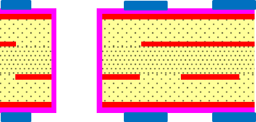 (Cross-section after Lamination & Development)
5.2 Precision Killers: Alignment & Side Etch
5.2.1 Alignment & Annular Ring
This is the geometric tolerance issue most easily overlooked by Layout Engineers.
- Collision of Mechanical vs. Optical: Drilling is a mechanical action, and the board undergoes expansion and contraction (Scaling, due to heat and moisture); Exposure is an optical action, and the film also scales. The two rarely overlap perfectly.
- Layer-to-Layer Registration: When you draw a 0.2mm hole in the exact center of a 0.4mm pad in CAD, you expect a uniform 0.1mm copper ring (Annular Ring) all around.
- Cruel Reality: The drill might shift left by 0.05mm, and the exposure film might shift right by 0.05mm. The result is that the ring width on one side becomes 0, or the drill even breaks out of the pad edge (Breakout).
- IPC Class 2 vs. Class 3 Differences:
- Class 2: Allows 90° Breakout, provided there is still connection between the hole wall and the pad. This is usually acceptable for mobile phones and consumer electronics.
- Class 3: Strictly requires No Breakout. Typically requires preserving at least 2mil (0.05mm) of external solid annular ring and 1mil (0.025mm) internal. This means Class 3 Pad designs must be significantly larger than Class 2, forcing a reduction in Routing Density.
5.2.2 Light Source Selection: LDI vs. Collimated Light
- Collimated Light: Uses high-pressure mercury lamps and film. If the light isn't perfectly parallel (large scattering angle), light can creep under the edge of the black film, causing under-exposure or over-exposure at the bottom of the dry film (slanted sidewalls). Resolution is limited for fine lines (< 4mil).
- LDI (Laser Direct Imaging): Does not use film; scans directly on the dry film with a UV laser.
- Advantage: LDI's greatest strength is Non-linear Scaling Compensation. It can read the actual position of the drilled targets on the board, calculate the board's deformation (e.g., trapezoidal or fan-shaped distortion), and dynamically adjust the circuit pattern to match the drilling. This is essential for HDI and high-density boards, but implies higher processing costs (equipment depreciation, slower speed).
5.2.3 Etch Factor & Trapezoidal Traces
Etchant is sprayed from top to bottom. As it bites vertically through the copper layer, it also etches sideways (Side Etch / Undercut).
- Trapezoidal Effect: The final trace cross-section is not a rectangle, but a trapezoid. Bottom width > Top width.
- Impedance Control Disaster: Many R&D engineers use a rectangular model when calculating impedance. However, at high frequencies (e.g., PCIe 5.0, 32Gbps), the trapezoidal cross-section reduces the effective conductor area, causing impedance to read high.
- Etch Factor Calculation: CAM engineers will pre-thicken the traces on the film based on the F value (Compensation). For example, if you want a 4mil trace, they might draw 4.5mil on the film to offset the loss from side etching.
5.3 eCloud DFM Advice for Layout/RD (Exposure & Impedance Section)
- The Redemption of Teardrops:
- Why: Not just for aesthetics. When misalignment occurs between drilling and the pad, teardrops provide extra copper connection area, preventing the drill from severing the Junction between the trace and the pad.
- Stress Relief: Teardrops also relieve stress at the trace root caused by hole wall expansion during thermal cycling, reducing micro-crack risks. Most CAM software now adds teardrops automatically; Layout Engineers should allow this in their design rules.
- The Cost Ladder of Trace/Space:
- 3mil/3mil processes are significantly more expensive than 5mil/5mil. Not only due to equipment requirements (needs LDI) but because yield is extremely sensitive to Particles. A 10 µm dust particle is just a nick on a 10mil trace, but it causes an Open on a 3mil trace.
- Takeaway: Unless necessary (like BGA fan-out), try to keep trace/space above 5mil (0.127mm).
- Annular Ring Design Principles:
- Set Pad Size according to factory capabilities. Generally, Pad diameter should be at least 10-12mil (0.25-0.3mm) larger than the Drill diameter. This guarantees that after all tolerance stacking, there is still at least 1-2mil of solid copper ring left, meeting IPC Class 2 or even Class 3 requirements.
6. Summary & Call to Action
The manufacturing process of a PCB is a precision symphony of physics, chemistry, and optics. Looking at the microscopic world:
- PTH solves the "Connectivity" problem through Palladium activation and autocatalytic redox, but is limited by Aspect Ratio and Desmear quality.
- Plating solves the "Copper Thickness" problem through the interplay of current density and organic additives, constantly fighting the "Dog-bone" effect.
- Exposure & Etching solve the "Pattern" problem through photochemical reactions and dynamic compensation, facing challenges in Alignment accuracy and Etch Factors.
Final Advice for Engineers:
- Don't Over-design: If you can use a 0.3mm hole, don't use 0.2mm. If you can use a 6mil trace, don't use 4mil. Every limit parameter eats away at your yield and increases cost.
- Understand Factory Language (EQ): When the Fab House raises an EQ (Engineering Question) asking to add teardrops, modify hole tolerances, or add dummy copper, please understand they are trying to save your board, not cause trouble.
- FA Mindset (Failure Analysis): Next time a via fails, don't just re-solder. Slice it open (Cross-section). Is it hole wall separation (Chemistry/Desmear issue)? Is it corner cracking (Stress/Plating issue)? Or is it CAF (Material/Drilling issue)? Only by finding the root cause can you avoid these pitfalls at the design source.
Interactive Question:
"As a Layout Engineer, have you ever encountered a 'Ghost Story' where the trace width met design specs, but impedance was way off? This was likely due to the trapezoidal effect caused by the Etch Factor being ignored. Feel free to share your 'board explosion' experiences and lessons learned!"
