Chapter 1: Introduction: The "Skin" Philosophy in PCB Manufacturing
In Taiwan's thriving electronics industry, the Printed Circuit Board (PCB) is hailed as the "Mother of Electronics." However, for many R&D engineers (RD) buried in schematics and layout designs, the physical manufacturing process of a PCB often remains a "black box" shrouded in mist. When we draw a trace or place a pad in CAD software, do we truly understand how these geometric shapes are transformed into physical entities in the factory?
Among these processes, Surface Finish is the most critical interface connecting "Design" and "Manufacturing." It is not only a protective coat for the copper foil but also a decisive factor in the success of Surface Mount Technology (SMT) assembly. If we compare a PCB to the human body, the copper foil is the blood vessels, the substrate is the skeleton, and the surface finish is the skin. The health of this skin directly determines whether the body can resist external oxidation and establish a good connection with the outside world (electronic components).
This report aims to provide a detailed, in-depth, and practical technical guide for Taiwanese electronics engineers, PCB Layout engineers, and electromechanical students. We will move beyond textbook definitions to explore the rivalry between the two mainstream processes: Hot Air Solder Leveling (HASL) and Electroless Nickel Immersion Gold (ENIG). We will dissect the chemical mechanism of "Black Pad Syndrome," uncover the secret behind the dominance of "Green Solder Mask," and re-examine surface finish selection strategies from the perspective of high-frequency Signal Integrity (SI).
Chapter 2: The Hegemony of Green: The Science and Myth of Solder Mask
When you pick up a PCB, what usually greets your eyes is a sea of green. Why not blue, red, or purple? This is not just an aesthetic habit, but the result of the combined effects of materials science, optical physics, and economics.
2.1 Why are most boards green? (The Hegemony of Green)
In the PCB industry, green solder mask occupies an absolute dominant position, with a market share exceeding 90%. This phenomenon is not accidental but an evolutionary result based on several core factors.
2.1.1 Visual Inspection and Human Ergonomics
Before the widespread adoption of Automated Optical Inspection (AOI), PCB quality inspection relied heavily on manual visual inspection. Based on the physiological structure of the human retina, the human eye is most sensitive to green light with a wavelength of approximately 500-570nm.1
- Contrast Advantage: Green solder mask forms the highest visual contrast against golden copper pads (or gold-plated pads), silver HASL pads, and white silkscreen text. This makes it easier for inspectors to identify shorts, opens, scratches, or foreign objects.
- Anti-Fatigue: Compared to red or blue, staring at green for long periods is less likely to cause visual fatigue, which is crucial for Quality Control (QC) personnel who spend their days looking through microscopes.
2.1.2 Cost Efficiency and Economies of Scale
This is a typical "Matthew Effect": because many people use green, production volume is high; because volume is high, costs are low; because costs are low, even more people choose it.
- Procurement Cost: The cost of green ink is typically 20% lower (or more) than other special colors. For consumer electronics where profit margins are calculated down to the penny, this is an advantage that cannot be ignored.
- R&D Investment: Ink suppliers (such as Taiyo Ink) invest the majority of their R&D resources into improving green formulas. Therefore, green ink usually has the widest process window, shortest curing time, and best chemical resistance.
2.1.3 Chemical and Physical Properties
- Resolution: Solder mask is defined through an exposure and development process. Green ink is optimized for UV light absorption and penetration, allowing for the creation of the finest "Solder Dams." In contrast, black ink absorbs a large amount of UV light, leading to incomplete curing at the bottom (undercure); white ink reflects UV light, leading to side erosion or poor resolution.
2.2 The Challenge of Black Solder Mask (The Dark Side)
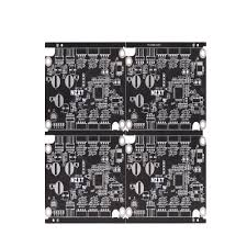
Although black PCBs are seen as a symbol of "high quality," "professionalism," and "mystery" in high-end consumer electronics (like Apple products and high-end gaming motherboards), for process engineers, black is simply a nightmare.
2.2.1 Blind Spots in AOI Inspection
AOI machines use light reflection to judge solder joint quality.
- Light Absorption: Black solder mask absorbs most incident light, causing the contrast between the background and the solder joints to drop drastically. AOI equipment struggles to distinguish between the copper surface and the substrate, leading to a high rate of false calls, forcing factories to increase manual re-inspection and lowering production efficiency (UPH).
- Thermal Management Disaster: According to black-body radiation laws, black objects are excellent heat absorbers. In a reflow oven, black PCBs absorb radiant heat much faster than light-colored PCBs. This can cause the board temperature to rise too quickly, potentially exceeding the thermal limits of sensitive components (like electrolytic capacitors or certain ICs) or exacerbating board warpage.
2.2.2 Potential Electrical Risks
- Conductivity Concerns: To achieve a deep black color, some low-end ink formulas add Carbon Black or Cobalt compounds. If trace amounts of these conductive substances remain, they can cause micro-leakage currents in high-voltage circuits or even affect impedance control, increasing the risk of short circuits. Therefore, high-voltage power supply boards rarely use black solder mask.
2.3 White Solder Mask: The Double-Edged Sword of the LED Industry
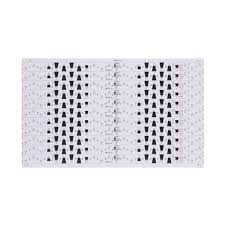
White solder mask is the standard configuration for LED lighting and backlight modules because its high reflectivity significantly increases lumen output. However, white ink faces severe "discoloration" issues.
2.3.1 Discoloration Mechanisms
White ink typically uses Titanium Dioxide (TiO2) as a white pigment.
- Thermal Discoloration: After enduring the high temperatures of SMT reflow (approx. 240-260°C), white ink tends to yellow or turn pinkish. This is due to the oxidation of the resin base or residue from photoinitiators.
- Chemical Contamination: If the ENIG process is used, chemicals from the nickel tank that are not cleaned off can remain on the white surface, appearing as unsightly yellow-brown spots after baking.
- Consequences: Discoloration affects not only appearance but also reduces reflectivity, leading to color shift in LED products—a taboo for optical products.
Chapter 3: Surface Finish Showdown: HASL vs. ENIG
This is the soul-searching question every hardware engineer must face when creating a BOM: choose the cheap and durable HASL, or the flat and noble ENIG? This is not just a cost issue, but a deep understanding of product reliability and application scenarios.
3.1 Hot Air Solder Leveling (HASL)
HASL is the oldest and most mature surface finish process in the PCB industry. Despite the emergence of new technologies, HASL still holds half the market due to its unmatched solderability.
3.1.1 Process Principle
The HASL process is quite intuitive and robust:
- Flux Application: The bare copper board is dipped in flux.
- Solder Dipping: The entire PCB is vertically immersed in a molten solder bath (temperature approx. 250-260°C).
- Air Knife Leveling: As the board is pulled up from the solder bath, two high-pressure hot air knives blow across the surface, removing excess solder and leveling the solder remaining in holes and on pads.
3.1.2 Advantages
- King of Solderability: Since the surface is essentially solder itself (Tin-Lead or Tin-Copper alloy), the fusion between solder paste and the pad surface during SMT reflow is "homogeneous fusion." There are absolutely no material interface barriers. Wetting is excellent, and non-wetting phenomena almost never occur.
- Cost-Effective: HASL equipment is relatively simple, raw materials (tin) are cheap, and the process speed is fast, making it the lowest-cost surface finish currently available.
- Reworkability: If plating defects (like exposed copper) are found during processing, the board can simply be cleaned and passed through the HASL machine again to be repaired. This is something chemical platings (like ENIG) cannot match.
- Long Shelf Life: The thick solder layer offers excellent physical protection against oxidation, with a shelf life of 12 months or more.
3.1.3 Disadvantages and Limitations
- Poor Surface Planarity: This is HASL's fatal flaw. Due to gravity and the surface tension of liquid tin, the pad surface becomes "dome-shaped."
- Consequence: For Fine Pitch components (like BGA, CSP, or QFN with Pitch < 0.5mm), solder balls can easily slide off the dome, causing misalignment; or uneven tin thickness can lead to bridging or open circuits.
- Thermal Shock: The PCB must be dipped directly into a 260°C solder bath.
- Consequence: This is a massive thermal shock to the board, easily causing thin boards (< 0.8mm) to warp, or even causing delamination or via cracking in multilayer boards.
- Bridging Risk: For very fine leg pitches (like QFP), the air knives may fail to blow away all residual solder between adjacent pads, creating solder bridges.

3.2 Electroless Nickel Immersion Gold (ENIG)
As electronic components have miniaturized, HASL's unevenness became a bottleneck, leading to the rise of ENIG as the synonym for high-end boards.
3.2.1 Process Principle
ENIG is a chemical displacement process requiring no electricity:
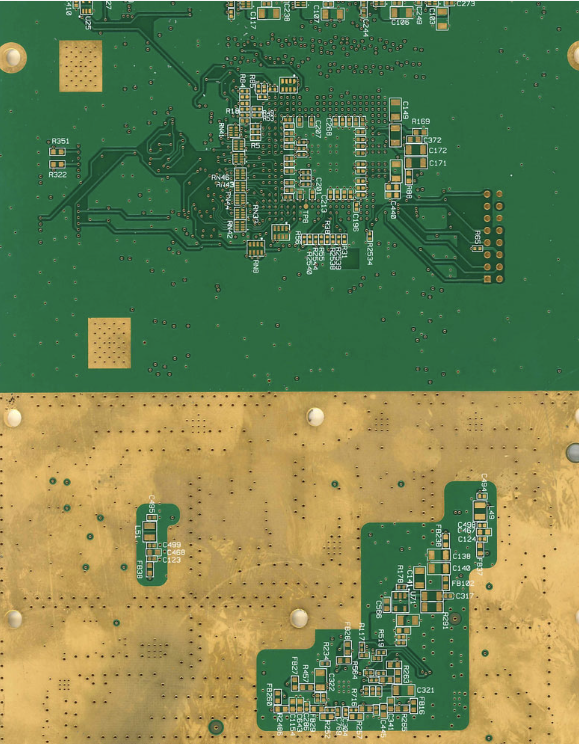
- Electroless Nickel: Using hypophosphite as a reducing agent, a Nickel-Phosphorus alloy layer (approx. 3-6 µm thick) is auto-catalytically deposited on the copper surface. This nickel layer is the main body for soldering, responsible for forming Intermetallic Compounds (IMC) with the solder paste.
- Immersion Gold: Utilizing the potential difference between nickel and gold, a displacement reaction occurs. Gold ions steal electrons from nickel atoms to reduce into gold metal, depositing on the nickel surface in an extremely thin layer (approx. 0.05-0.15 µm / 2-5 µin). The gold layer serves only to protect the nickel from oxidation. During soldering, the gold quickly dissolves into the solder paste, exposing the nickel layer for soldering.
3.2.2 Advantages
- Excellent Planarity: The chemically deposited thickness is very uniform, and the surface is mirror-flat. This is critical for mounting microscopic passive components like 0201 or 01005, and Fine Pitch BGAs, significantly improving SMT yield.
- Corrosion Resistance & Contact Resistance: Gold is an inert metal with strong oxidation resistance. This makes ENIG the preferred choice for keypad contacts, Gold Fingers (though Hard Gold is better for wear, ENIG works for low insertion cycles), and conductive glue interfaces.
- Heat Tolerance: ENIG can withstand multiple reflow cycles, making it suitable for double-sided SMT processes.
3.2.3 Disadvantages and Limitations
- Black Pad Syndrome: This is ENIG's most famous failure mode and a nightmare for engineers. It causes solder joints to become extremely brittle, breaking under stress (see Chapter 4).
- High Cost: The process is complex (involving degreasing, micro-etching, acid pickling, activation, nickel plating, gold plating, and multiple washes), and gold is expensive, resulting in costs 30-50% higher than HASL.
- Signal Loss: Nickel is a ferromagnetic material, which generates magnetic loss at high frequencies, affecting Signal Integrity (see Chapter 5).
3.3 Decision Matrix: How Should Engineers Choose?
To facilitate quick decision-making for RDs, we have compiled the following comparison table:
| Feature | HASL / LF-HASL (Spray Tin) | ENIG (Immersion Gold) | OSP (Organic Solderability Preservative) |
| :--- | :--- | :--- | :--- |
| Cost | Low | High | Very Low |
| Surface Flatness | Poor (Dome shape) | Excellent (Flat) | Good (Flat) |
| Solderability | Excellent (Homogeneous) | Good (Beware Black Pad) | Good (Fear of oxidation) |
| Shelf Life | Long (>12 months) | Long (>12 months) | Short (3-6 months) |
| Thermal Shock (Mfg) | High (260°C dip) | Low (Chemical reaction) | Low |
| Reflow Cycles | Multiple (Heat resistant) | Multiple | Limited (Film degrades) |
| Signal Integrity (HF) | Poor (High roughness) | Medium (Nickel magnetic loss) | Excellent (No extra metal) |
| Fine Pitch Components | Not Recommended (<0.5mm risky) | Highly Recommended | Recommended |
| Major Defects | Bridging, uneven thickness, warpage | Black Pad Syndrome | Oxidation/Reflow wetting issues |
| Typical Applications | Power boards, Backplanes, Low-end Consumer | Smartphones, Laptops, BGA Carriers | Motherboards, Servers, RF Boards |
Chapter 4: The Silent Killer: Black Pad Syndrome
If HASL's downsides are "visible" (unevenness seen by the naked eye), ENIG's downsides are "invisible" and fatal. Black Pad Syndrome usually causes solder joint fractures after the product has shipped, triggered by transport vibration or thermal expansion, leading to catastrophic market returns.
4.1 The Mechanism: A Runaway Chemical Reaction
The root cause of Black Pad lies in the uncontrolled displacement reaction between nickel and gold, leading to the collapse of the nickel surface structure.
- Hyper-Corrosion:
If the gold bath activity is too aggressive, or the nickel layer's crystal structure is loose (clear grain boundaries), the gold solution will corrode downwards along the nickel grain boundaries like acid rain, creating deep corrosion channels (Mud Cracks).
- Formation of Phosphorus-Rich Layer:
The electroless nickel layer is not pure nickel but a Nickel-Phosphorus alloy (Ni-P), typically containing 7-10% phosphorus. In the displacement reaction, gold replaces nickel but not phosphorus. As nickel is dissolved, the remaining phosphorus atoms accumulate at the nickel-gold interface, forming an ultra-thin but highly concentrated "Phosphorus-Rich Layer" (P-rich layer).
- Brittle Fracture:
This P-rich layer has extremely poor mechanical strength and cannot form a good alloy with solder paste. When the solder joint solidifies and generates internal stress, or is subjected to external force (like a Drop Test), the joint does not break through the solder (Ductile Fracture) but peels directly off this fragile P-rich layer, leaving a black, oxidized nickel surface—hence the name "Black Pad".
4.2 Is Black Pad Caused or Revealed by Reflow?
This is a common misconception. Black Pad is formed during the PCB manufacturing process (ENIG plating), not during SMT reflow.
- SMT reflow thermal stress simply "reveals" this defect.
- When solder paste melts and wets the gold surface, the gold dissolves rapidly, exposing the underlying nickel. If the nickel layer is already corroded and black (nickel oxide), the solder cannot wet the nickel, causing non-wetting or "Cold Joints" with very weak adhesion.
- In some cases, the joint looks good, but detaches with slight force, revealing a black interface—a classic Black Pad signature.
4.3 How to Prevent and Detect?
Engineers at the design stage find it hard to completely prevent Black Pad as it is a process control issue at the PCB fab. However, RDs can manage risk by:
- Specifying Medium Phosphorus Nickel: Confirm with the fab that their nickel bath phosphorus content is controlled at 7-10%.
- Phosphorus < 7% (Low Phos): Poor corrosion resistance, easily attacked by gold bath, high Black Pad risk.
- Phosphorus > 10% (High Phos): Good corrosion resistance, but poor solderability and high plating stress.
- Strict Gold Thickness Control: Gold should not be too thick. Although gold is expensive, some customers mistakenly think "thicker is better." In reality, thicker gold means longer displacement reaction time, increasing the risk of nickel corrosion. IPC-4552 recommends gold thickness be controlled at 2-4 µin (0.05-0.1 µm).31
- Destructive Analysis: In the Approval Sheet stage, require the fab to provide Cross-section and SEM (Scanning Electron Microscope) reports to check the Ni-Au interface for "Mud Cracks" or corrosion spikes.
Chapter 5: The Invisible Killer of High-Frequency Signals: Skin Effect and Insertion Loss
For RDs designing 5G, Millimeter-wave radar, or high-speed Servers, the choice of surface finish is no longer just about soldering, but about Signal Integrity (SI). Here, a counter-intuitive phenomenon arises: The premium-looking ENIG often performs worse at high frequencies than the cheap OSP or Immersion Silver.
5.1 The Physics of Skin Effect
When AC flows at high frequencies, the current tends to concentrate on the surface of the conductor, with almost no current in the center. This is the Skin Effect. The higher the frequency, the shallower the depth of current flow At 1 GHz, the skin depth of copper is approx. 2 µm.
- At 10 GHz, the skin depth is only approx. 0.66 µm.
5.2 Magnetic Interference of the Nickel Layer
In the ENIG process, the copper is covered by approx. 3-5 µm of nickel.
- High Resistivity: Nickel's resistivity is about 4 times that of copper.
- Ferromagnetism: This is critical. Nickel is magnetic, and its relative permeability is far higher than copper (Copper ).
When high-frequency signals (e.g., 10 GHz) flow through an ENIG surface, since the skin depth is less than the nickel thickness (0.66 µm < 3 µm), most of the current is forced to flow through the high-resistance, magnetic nickel layer instead of the low-impedance copper. This causes a drastic increase in Insertion Loss.
5.3 Data Speaks: ENIG vs. HASL vs. Immersion Silver
Research shows that in bands above 10 GHz:
- ENIG: Highest loss. Loss per inch can increase by 0.2 to 0.5 dB compared to bare copper. This is unacceptable for 5G systems with tight Link Budgets.
- HASL: Although tin is less conductive than copper (approx. 1/7th), it is non-magnetic. However, HASL surfaces are extremely rough. According to electromagnetic theory, rough surfaces lengthen the signal path (current must travel over "hills and valleys"), increasing loss and causing Impedance Mismatch.
- Immersion Silver / OSP: The best choices for high-frequency boards.
- Immersion Silver: Silver has the best conductivity (better than copper) and is non-magnetic. The layer is thin (0.2-0.4 µm), allowing current to flow smoothly.
- OSP: An organic film that evaporates during soldering, leaving signals to travel directly on copper.
- Both provide signal performance close to bare copper with excellent surface flatness.
Engineer's Advice:
- Freq < 1 GHz: ENIG is safe and offers stable impedance.
- Freq > 5-10 GHz: Avoid ENIG. Use Immersion Silver, Immersion Tin, or OSP.
- RF Design Trick: If ENIG is mandatory (e.g., for wear resistance), consider "ENEPIG" (Nickel-Palladium-Gold) or thin-nickel processes. Alternatively, open the Solder Mask over RF lines and specify Selective Plating (no nickel on RF traces), though this increases manufacturing complexity.
Chapter 6: The Writing on the Board: A Practical Guide to Silkscreen
Silkscreen (Legend) does not affect circuit function but is vital for SMT loading, manual insertion, and debugging. A common mistake by Taiwanese RDs is shrinking text too much for aesthetics or density, leading to blurred or illegible text.
6.1 Minimum Size Limits: Don't Challenge Physics
PCB text printing is divided into Traditional Screen Printing and Direct Legend Printing (DLP/Inkjet).
6.1.1 Screen Printing
The traditional method uses a mesh to print ink.
- Limit: Constrained by mesh tension and ink bleeding. Low resolution.
- Capability: Usually requires Line Width 6 mil (0.15mm), Text Height 32-40 mil (0.8-1.0mm). Below this, text blobs or breaks.
6.1.2 Direct Legend Printing (DLP)
Modern factories use DLP, similar to an inkjet printer. High resolution and automatic registration.
- Capability: Can reach Line Width 4-5 mil, Text Height 25-30 mil.
6.1.3 Recommended Safe Values (IPC-7351 Reference)
To ensure clarity across all factories (including lower-tier ones), standard Layout rules are:
- Min Line Width: 6 mil (0.15mm). Below this, lines may break or ghost.
- Min Text Height: 40 mil (1.0mm). This ensures comfortable readability.
- Aspect Ratio: Keep the stroke width proportional to height (e.g., 1:6 or 1:8) to avoid text becoming a blob of ink.
6.2 DFM (Design for Manufacturing) Pitfalls
- Do not print on Pads: The most basic rule. Ink is an insulator. If printed on a pad, it blocks solder paste from contacting copper, causing Solder Skips or poor connections. Even if CAM software cuts it, RDs should avoid this in design.
- Discoloration after Soldering: White text may yellow slightly after HASL or Reflow temperatures. This is normal as long as it doesn't char or peel.
- Text over Vias:
- If printed on an unfilled via, ink leaks into the hole, breaking the text.
- If printed on plugged vias, the uneven surface distorts the text.
- Countermeasure: Use the "Clip Silkscreen" function when generating Gerbers to automatically remove text over Vias or Pads.
Chapter 7: Solder Defect Analysis: It's Not Just the Surface Finish's Fault
When production reports defects, RDs often blame the surface finish first. However, many defects result from the interaction of Design (Layout) and Process parameters.
7.1 Tombstoning (Manhattan Effect)
Phenomenon: One end of a small chip component (0402, 0201) solders well, while the other lifts up, standing vertically like a tombstone, causing an open circuit.
Causes:
- Wetting Imbalance: Uneven heating or solder paste volume on pads. The end that melts first generates strong Surface Tension, pulling the component upright if the other end hasn't melted or has less pull.
- Layout Issue: One pad connects to a large copper plane (heatsink effect, slow heating), the other to a thin trace (fast heating).
- Surface Finish Impact:
- HASL: Due to the dome shape, components slide easily, increasing tombstoning risk.
- ENIG: Extremely flat with low friction. If placement pressure is wrong or flux activity is too high, components can "swim" and tombstone during melt.
Countermeasure: Use Thermal Relief pads to balance heat capacity; for ENIG, precisely control Reflow soak zones.
7.2 Cold Solder
Phenomenon: Solder joints look dull, grainy, rough, and lack a proper Alloy Layer (IMC). Strength is poor.
Causes:
- Insufficient Heat: Reflow peak temp too low or Time Above Liquidus (TAL) too short.
- Oxidation: Pad surface is heavily oxidized, blocking tin-copper diffusion.
- Surface Finish Impact:
- HASL: Rarely cold solders unless storage was terrible (deep oxidation).
- OSP: If OSP film degrades from moisture or multiple reflows, copper oxidizes rapidly, causing cold solder.
- ENIG: If Black Pad occurs, solder cannot wet the nickel, creating a "Cold Joint" look-alike.
7.3 Solder Wicking
Phenomenon: Molten solder flows down a Via, leaving insufficient solder on the pad, potentially causing opens.
Causes:
- Via-in-Pad: Placing a via directly in a pad without plugging or plating it over (POFV).
- Capillary Action: Molten solder is sucked into the hole.
Countermeasure:
- Layout: Avoid vias in small pads. If necessary, use a "Dog bone" trace fan-out.
- Process: Use VIPPO (Via-in-Pad Plated Over) technology: plug via, plate flat, then apply ENIG.
Chapter 8: Conclusion and Future Outlook: The Last Mile to Reliability
8.1 Comprehensive Advice: The RD's Decision Tree
For Taiwanese R&D teams, follow this logic when selecting surface finishes:
- Consumer Electronics / Cost Sensitive / Wide Pitch (>0.5mm) / DIP Components:
- Choice: HASL (Lead-Free).
- Reason: Cheap, robust, high yield, easy rework. Unevenness is not an issue for large parts.
- HDI / BGA / QFN / Fine Pitch (<0.5mm):
- Choice: ENIG.
- Reason: Flatness is mandatory for yield. Despite Black Pad risk, it is manageable with mature fab process control.
- High-Frequency RF (>5 GHz) / 5G / mmWave:
- Choice: Immersion Silver or OSP.
- Reason: Avoids nickel's magnetic loss and skin effect. Immersion Silver offers better conductivity/contact than OSP.
- Keypads / Gold Fingers / Conductive Glue:
- Choice: ENIG or Hard Gold.
- Reason: Wear resistance, oxidation resistance, stable contact resistance.
8.2 Future Trends: ENEPIG and EPIG
Facing Black Pad issues and High-Frequency needs, the industry is moving towards:
- ENEPIG (Nickel-Palladium-Gold): Adds a Palladium layer (approx. 0.05-0.1 µm) between Nickel and Gold.
- Pro: Palladium prevents gold from corroding the nickel, eliminating Black Pad. Harder surface suitable for Wire Bonding.
- Con: Palladium is expensive; process is complex. Standard for high-end IC Substrates and Apple products.
- EPIG (Electroless Palladium Immersion Gold - No Nickel): Removes nickel entirely. Palladium on Copper, then Gold.
- Pro: The ultimate solution for RF. No magnetic nickel layer (Excellent Signal Integrity), retains noble metal stability.
PCB Surface Finish is a thin layer, mere microns thick, yet it embodies the profound science of inorganic chemistry, metallurgy, electromagnetics, and thermodynamics. For engineers, there is no "best" finish, only the "most suitable" for the design, budget, and environment. We hope this report serves as a powerful reference for your engineering decisions.
