February 25, 2026
In the field of PCB design, a debate has raged for two decades and remains a common point of friction between R&D departments and manufacturers: “Are teardrops a lifesaving structural safeguard, or poison for high-frequency signals?”

For process engineers in traditional PCB factories, teardrops are the guardians of yield. But for Signal Integrity (SI) experts tackling 112G SerDes or PCIe Gen 6, automatically adding teardrops across the entire board without simulation verification is often seen as a risky behavior that lacks bandwidth budget assessment.
This guide breaks away from the binary "add all" or "add none" mindset. Based on physical structure, IPC Class 3 specifications, and ultra-high-frequency simulation data, it establishes a data-driven teardrop decision framework for R&D engineers and design managers.
A teardrop refers to the extra conical or arc-shaped copper foil transition added at the junction where a trace enters a pad or via. This design is not for aesthetics; it provides three key values in manufacturing and long-term reliability.
Although modern CNC drilling equipment boasts high positioning accuracy, the substrate often undergoes micron-level expansion and contraction due to temperature, humidity, and pressure during multi-layer board lamination. If the drill bit deviates towards the trace connection side, it can easily cut through the narrow trace neck, scrapping the entire board. Teardrop design increases the "copper transition area," ensuring that even with a deviation of over 2 mils, sufficient electrical contact and physical strength are maintained between the trace and the hole wall. In HDI high-density board processes, this compensation method can effectively increase production yield by 3% to 5%.
The Coefficient of Thermal Expansion (CTE) of PCB resin materials (like FR-4) in the Z-axis direction is approximately 50-80 ppm/°C, much larger than that of metallic copper at 17 ppm/°C. During temperature rise cycles in reflow soldering or system operation, the via structure acts like a piston, violently pulling on the connected trace. Fine lines below 5 mils without teardrop reinforcement are prone to micro-cracks at the junction or even "Pad Lifting." Experimental data shows that teardrop designs with a 0.2mm gradual transition zone can reduce the peak stress caused by thermal expansion mismatch by about 35%.
During the chemical etching process, etchant can easily get trapped in the 90-degree sharp corners between traces and pads. If not cleaned properly, this not only leads to over-etching in that area, thinning the trace, but can also cause long-term latent corrosion failure. Teardrops smooth out sharp angles, allowing process chemicals to flow more uniformly, which is fundamental for high-precision impedance control boards.
When data rates cross into the 112G PAM4 era (Nyquist frequency 28 GHz), every femtofarad (fF) of capacitance change can affect the eye diagram opening. The side effects of teardrops on signal integrity cannot be ignored.
The additional copper area introduced by teardrop design increases parasitic capacitance to the reference ground plane. In controlled impedance transmission lines, this creates a distinct low-impedance point.
Practical Observation: In frequency bands exceeding 10 GHz, unoptimized teardrop designs can cause a noticeable increase in Insertion Loss, and depending on the project's stack-up structure, the impact can exceed 0.5dB.
Many EDA tools' automated teardrop functions lack symmetry awareness. When routing space is tight, the software might generate a teardrop on only one end of a differential pair, or the generated teardrops on both sides may have inconsistent geometries.
This "geometric asymmetry" introduces phase Skew, causing asymmetric closure of the three vertical eye diagrams for PAM4 signals, thereby worsening the system's Bit Error Rate (BER).
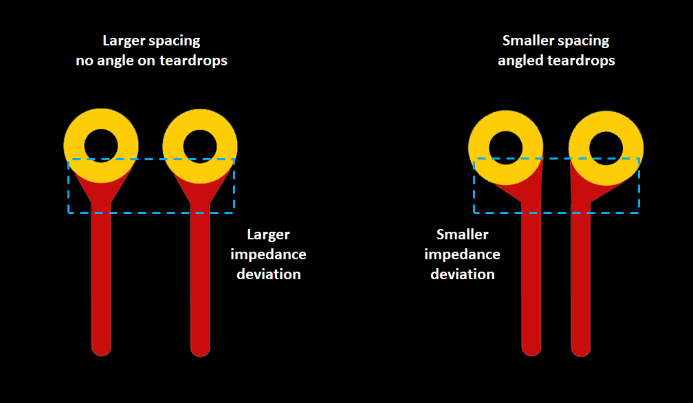
At eCloud, we emphasize decision-making based on bandwidth budget, rather than automated one-click generation for the entire board.
Teardrop Application Strategy Table (Bandwidth-Based Strategy)
| Application Scenario / Frequency | Impedance Dip Risk | Teardrop Recommendation | Core Execution Guidelines | | :--- | :--- | :--- | :--- | | < 5 GHz (Low Speed / General Digital) | Low | Add Everywhere | Prioritize mechanical reliability and manufacturing yield. | | 5 – 25 GHz (PCIe 4.0/5.0) | Medium | Add Locally & Controllably | Add only for fine traces, strictly ensure differential pair symmetry. | | > 25 GHz (112G / PCIe 6.0) | Extremely High | Add Only After 3D Simulation | Automated teardrops without simulation are strictly prohibited. Adjust the transition zone manually. |
Advanced SI Solution: Controlled Taper Theory
For ultra-high-speed links above 112G, we recommend using controlled tapers (like the Klopfenstein impedance profile). This is no longer simply "adding copper," but precisely calculating the logarithmic curve of conductor width variation. It transforms the teardrop from a physical reinforcement structure into a precise "broadband impedance transformer" to compensate for the capacitive effects of vias.
For failure-intolerant fields like aerospace, medical, or automotive electronics, teardrops are often a key tool to meet regulatory requirements.
According to IPC-6012F:
In Class 3 designs, if high routing density leaves limited space on the pad, teardrops are often used as a primary engineering method to increase the Annular Ring compensation margin. In this context, adding teardrops is not just for reliability; it's to ensure the product passes rigorous cross-section analysis and meets international compliance standards.
Instead of dealing with solder joint fractures or signal distortion after prototyping, stick to these five red lines during the layout stage:
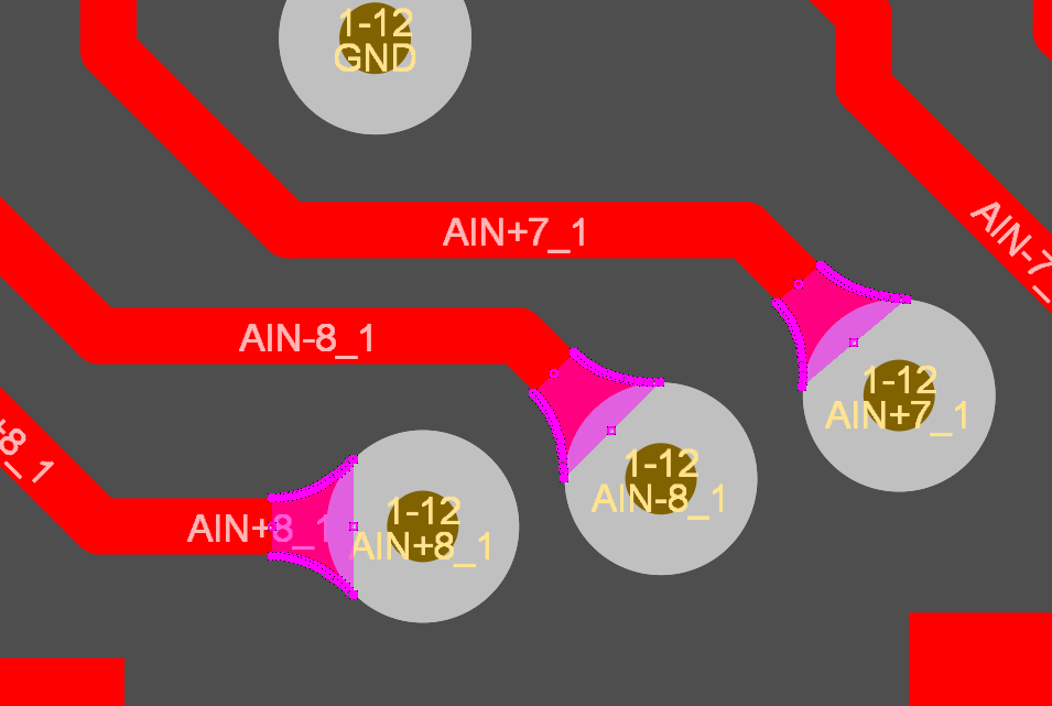
In high-end projects at YiYun Technology (eCloud Technology), we treat teardrops as part of precision engineering.
For link designs above 112G, we do not adopt a "blind reinforcement" approach. Instead, we perform 3D EM (ANSYS HFSS) full-wave simulations on critical differential via transitions. By finely adjusting the Antipad geometry to precisely compensate for the parasitic capacitance introduced by the teardrop, we minimize impedance distortion at the physical level.
Remember: "In extreme manufacturing processes, only traceable data can end the debate." Blindly adding everywhere is a risk, but blindly adding nowhere is also a hidden danger. Only through based on the bandwidth budget can you build a true quality moat for your product, balancing DFM yield and SI performance.
If you are facing design dilemmas with ultra-high-speed routing, feel free to contact the eCloud DFM expert team. We are more than just a PCB supplier; we are your hardware development accelerator.
