March 31, 2026
As part of our commitment to providing expert-level services for high-speed PCBs, we frequently assist our clients in resolving various complex design challenges. In today’s technical column from eCloud, we’ll take a look at the 13 most commonly overlooked PCB layout errors in everyday design:
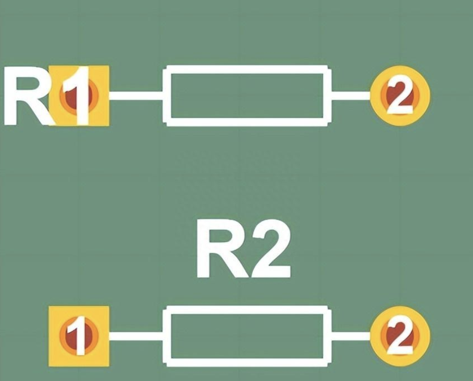
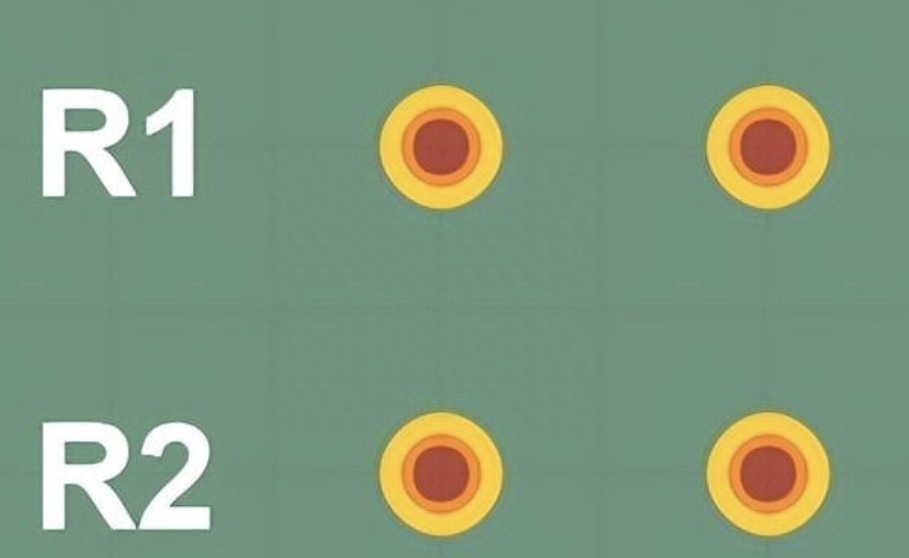
Reference Designators (RefDes) placed on copper foil are clearly visible in PCB layout software, but they become invisible after SMT assembly. Putting reference designators on pads causes many problems when placing or identifying components later.
In the figure below, the reference designator for R1 is not fully printed on the PCB, while R2 is placed correctly.
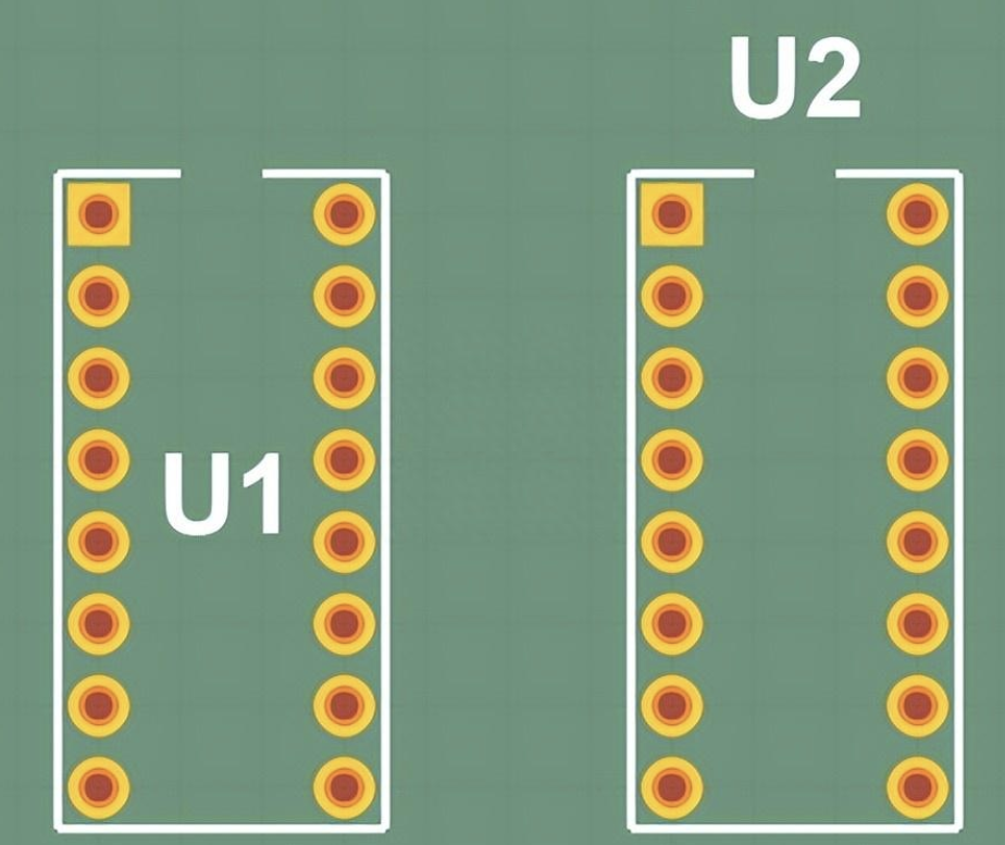
Putting reference designators underneath components may save space on the board, but if you later need to desolder, remove, or replace a component for debugging or repair, you cannot intuitively locate the part.
In the figure, after U1 is placed on the PCB, its reference designator is hidden; U2’s designator remains clearly visible.
Using thermal relief (also called cross‑shaped spokes) on component pads makes soldering easier. You might avoid thermal relief to reduce electrical and thermal resistance, but doing so makes soldering extremely difficult. Especially when a pad connects to a large copper area or copper pour, that large area acts as a heatsink, quickly wicking heat away from the soldering iron. Without proper thermal relief, you risk open or cold solder joints.
In the figure below, Q1’s source pad has no thermal relief, making soldering and desoldering inconvenient. Q2’s source pad has thermal relief, making both operations easier.

When designing a PCB with wireless functionality, an antenna is usually required on the board. Errors often occur when there is an impedance mismatch between the transceiver and the antenna. In such cases, maximum power transfer cannot be achieved, and the antenna will not work properly.
A proper microstrip line makes it easy to create a transmission line on the PCB and must be used to match the impedance between the antenna and the transceiver. In most cases, designing a 50Ω microstrip provides maximum power transfer. To achieve precise impedance control, designers must set the microstrip width according to the PCB’s dielectric specifications.
Some engineers habitually use the minimum allowable width for power traces without calculating the actual current they need to carry. For example, the default minimum width is often insufficient for a 500mA trace.
Trace width depends on whether the trace is on an outer or inner layer. Outer layer traces can carry more current than inner layer traces of the same thickness because they dissipate heat more easily into the air.
Decoupling capacitors provide stable power to the product. They must be placed as close as possible to the power pins they are stabilizing. If placed incorrectly, they may not function properly.
Always place decoupling capacitors near the power supply pins for best performance. Proper orientation and appropriate placement distance also improve transient response.
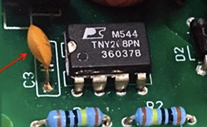
There are two main types of voltage regulators: linear regulators and switching regulators. Linear regulators are easy to layout and inexpensive, but they dissipate more power. Switching regulators are more complex but offer higher efficiency and lower power dissipation. Therefore, when laying out a PCB, you must strictly follow the layout guidelines in the datasheet.

Vias are used to connect different layers of a PCB. Through‑holes connect all layers (e.g., L1, L2, L3, L4). Blind vias connect an outer layer to an inner layer. Buried vias connect one inner layer to another inner layer.
The number of vias should be controlled to prevent them from increasing board size, as they consume routing space. Layers without vias can also be affected.
A common mistake is designing buried or blind vias that are difficult or impossible to manufacture. Buried and blind vias are more expensive than regular through‑holes, increasing total PCB cost. Also, designers must consider the limitations of each via type—for example, a buried via cannot connect Layer 1 (L1) and Layer 3 (L3).
Reference designators should be placed as close as possible to their associated components. If not, it becomes difficult to place the correct component in the correct location during assembly (SMT/DIP) and debugging. For example, without close placement, you cannot tell which is R1 and which is R2.
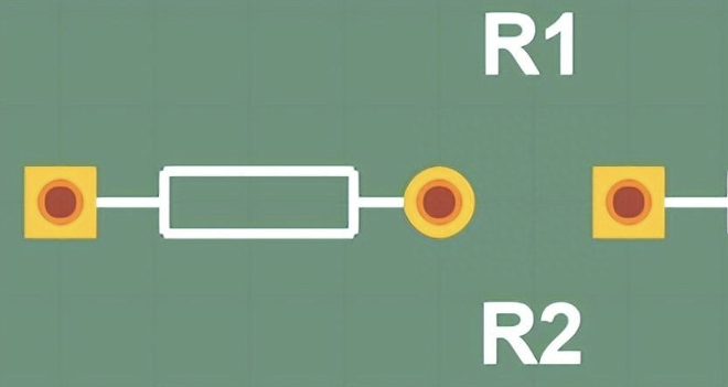
When adjacent components have reference designators that do not clearly indicate which pad belongs to which component, many problems arise. For instance, the wrong component may be placed on the wrong pad, or a component may be placed in an unintended orientation, causing shorts or opens.
In the figure below, the resistor should have been placed horizontally, but during assembly it was placed vertically, making the PCB inoperable. Using footprints with a silkscreen outline around the component prevents this problem.
Reference designators on a PCB should all face the same direction for easy reading. Random orientation makes debugging extremely painful. In the figure, the left side shows designators all facing the same direction, while the right side is disorganized.

There should be a clear indicator (dot, star, or similar) next to Pin 1 of an integrated circuit to ensure correct orientation during assembly. An incorrectly oriented IC may be damaged or even destroyed when powered on.
When the IC is soldered to the PCB, it is easier to inspect and debug if the Pin 1 indicator is not hidden under the component. In the figure, it is difficult to confirm whether U1 is oriented correctly. U2, however, is clearly correct because Pin 1 is clearly marked (square pad).

Many components are polarized. Incorrectly mounting a polarized component can cause circuit malfunction or component damage. An LED only lights when installed correctly. If reversed, it will not conduct and may be damaged by reverse voltage. An electrolytic capacitor can even explode under reverse bias. Always use footprints that indicate polarity. Polarity markings should not be hidden under the component.
In the figure, C1’s footprint is poor because the polarity marking is covered by the component itself. C2’s footprint is better because the polarity marking remains visible after the capacitor is soldered onto the PCB.

These are the 13 common PCB layout mistakes. Have you encountered any of these pitfalls in your designs?
