April 9, 2026
Electroless nickel-gold (ENIG), electroplated gold, nickel-palladium-gold (ENEPIG), and flash gold are all types of surface treatment for PCBs. Although the names all include the word “gold,” they differ significantly in terms of process principles, metal layer structure, and application scenarios. In this week’s technical column, we’ll provide a detailed analysis of their differences.
ENIG (Electroless Nickel Immersion Gold)
The full name is Electroless Nickel Immersion Gold. Through a chemical redox reaction, a layer of nickel is deposited on the copper surface, followed by a displacement layer of gold. It has extremely high surface flatness, making it very suitable for aluminum wire bonding and complex soldering. It is currently the most mainstream surface finish process in the industry.
Electroplated Gold
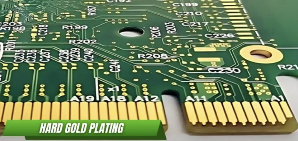
Nickel and gold are electroplated onto the copper surface using direct current. Electroplating allows for a thicker gold layer with high hardness and wear resistance. It is typically used for gold fingers, keypads, and other areas requiring frequent insertion/removal or physical contact.
Note: The process of electroplating the entire board is extremely expensive and may increase the risk of short circuits between gold traces.
ENEPIG (Electroless Nickel Electroless Palladium Immersion Gold)
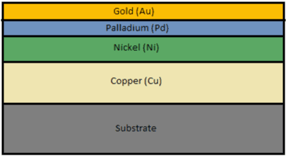
Can be seen as an “upgraded version” of ENIG, adding a palladium layer between the nickel and gold layers. The palladium layer completely blocks nickel migration, minimizing the risk of “black pad.” It also supports both gold and copper wire bonding and is mainly used for advanced packaging substrates (e.g., smartphone chip substrates).
Flash Gold
Typically refers to “electroplated thin gold” – after nickel plating, an extremely thin layer of gold (usually < 0.1 μm) is deposited. Its main function is to temporarily protect the nickel surface from oxidation. However, its solderability is poor, and it is mostly used for conductive keypads or low‑cost, quick‑turn prototyping.
This is the most mainstream process for BGA and fine‑pitch pads. The surface is very flat (beneficial for SMT assembly) and appears golden yellow. Because it is chemically deposited, the gold layer is extremely thin (approx. 0.05–0.1 μm). The primary purpose of the gold layer is to “protect the nickel layer from oxidation.”

Because it requires electrical current, “selective plating” is usually used; full‑board electroplating is rare. The gold thickness can be controlled, ranging from 0.25 μm to several micrometers. Hardness is mainly divided into two types: hard gold (doped with cobalt or nickel, very wear‑resistant) for mating contacts, and soft gold (99.99% pure gold) for wire bonding.
Primarily targeted at advanced packaging needs, solving the “black pad” problem of ENIG and the “high cost” of electroplated gold. The structure is Ni + Pd + Au. The palladium layer is an inert metal that serves as an excellent barrier.
The industry definition of “flash gold” can sometimes be ambiguous. It typically refers to one of two very thin gold layers: