April 14, 2026
In the field of high-end printed circuit board (PCB) manufacturing, the POFV (Plated Over Filled Via) process has become one of the key technologies for manufacturing high-density interconnect (HDI) boards. Commonly referred to in the industry as “cap copper,” this term vividly describes the process’s characteristic—much like carefully placing a “copper cap” on top of a resin-filled via. This technology not only resolves the issue of surface depression on traditional resin-filled vias but also provides a flat, reliable surface foundation for subsequent fine-line fabrication. It is an indispensable manufacturing process for today’s high-end electronic products, including servers, communication equipment, and aerospace applications.
POFV stands for Plating Over Filled Via. In the industry, it is also frequently referred to as VIPPO (Via in Pad Plating Over) or simply VIP boards.
Its specific definition is: a process design where a via is fully filled with resin, the protruding resin on the surface is planarized (ground flat), and then it undergoes electroless copper (PTH), electroplating, and etching processes to ultimately form a completely flat pad directly over the via.
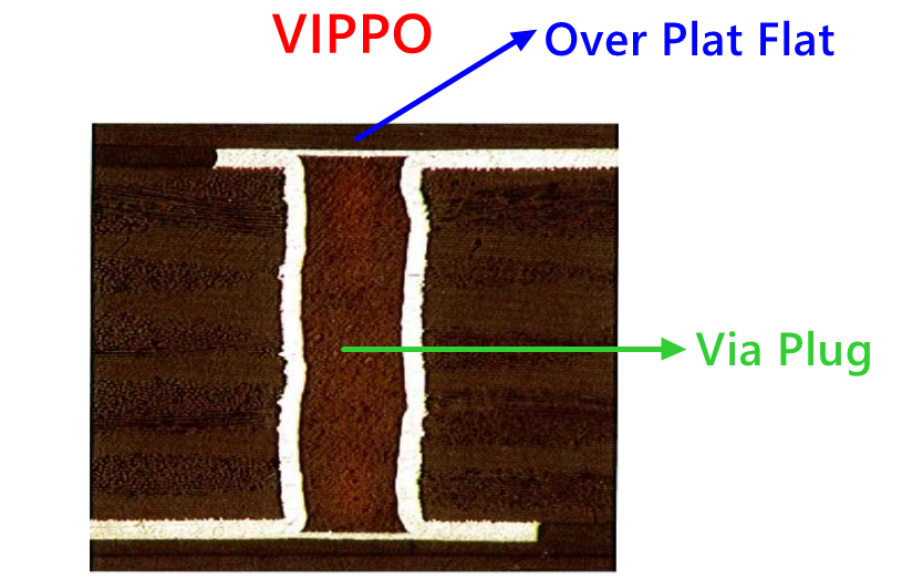
The POFV process begins with the creation of traditional through-holes or blind vias. After drilling, electroless copper (PTH) is applied to the hole walls to form a thin conductive layer, which is then thickened via panel plating. Subsequently, specialized equipment is used to plug a custom resin into the via. This step requires precise control of the filling volume to ensure the resin slightly protrudes above the board surface, leaving a margin for the subsequent planarization (grinding) step.
After the resin cures, an initial grinding process removes the excess resin, making the resin surface roughly flush with the copper foil surface. If the process were to stop here, it would merely be a traditional resin-plugged via. However, this surface has microscopic unevenness, and the adhesion between the resin and copper is limited, rendering it inadequate for the SMT assembly demands of high-end applications.

The true "capping" process begins with the second electroplating step. After roughening the surface of the resin-plugged via, a copper layer is deposited over the entire board surface via electroless copper and panel plating. This copper simultaneously covers the resin surface, forming the initial "Cap Copper" structure.
Precision control at this stage is vital:
Once the cap copper is formed, the subsequent flow varies depending on whether the manufacturer utilizes a "Positive Process" (Pattern Plating) or a "Negative Process" (Tenting/Panel Plating). However, the core objective remains the same: precisely forming circuit patterns while protecting the integrity of the cap copper.
According to international IPC standards, the Cap Copper thickness in the POFV process has strict classification requirements:
Note: These standards refer to the final thickness "before product shipment." During the actual manufacturing process, engineers must implement a "pre-compensation design" to offset the cap copper loss caused by subsequent micro-etching and planarization steps.
In the POFV process, choosing between the Negative and Positive processes primarily depends on "copper thickness requirements" and "line width capabilities," alongside a comprehensive consideration of in-house equipment compatibility.
| Consideration Dimension | Negative Process | Positive Process | | :--- | :--- | :--- | | Core Logic | Subtractive process (direct etching after panel plating) | Additive process (etching after pattern plating thickening) | | Process Advantages | Fewer steps, higher production efficiency, relatively lower equipment investment. | Thinner copper before etching favors fine-line resolution; Cap copper thickness can be independently thickened via pattern plating. | | Process Limitations | Extremely strict control over initial copper thickness required. Copper that is too thin causes via cracking during micro-etching; copper that is too thick makes etching fine lines difficult. | Complex flow, longer production cycle, higher costs, requires highly precise control of the pattern plating process. | | Copper Thickness Req. | < 15 μm, medium uniformity requirement | ≥ 12 μm, extremely high uniformity requirement | | Line Width/Space (L/S) | ≥ 50 μm (2 mil) | ≤ 50 μm (Under 2 mil) | | Reliability Level | IPC Class 2 | IPC Class 3 and above | | Applicable Products | Consumer electronics, general industrial control | High-end servers, telecom base stations, aerospace equipment |
Server-grade PCBs impose extremely stringent requirements on the POFV process:
To meet the above demands, the "Positive Process", combined with the following measures, is typically the preferred choice for high-end PCB manufacturers:
Copper thickness control in the POFV process is fundamentally an art of precise balance—finding the optimal solution among cost, performance, efficiency, and reliability. As the PCB industry rapidly trends toward higher density, higher frequencies, and higher reliability, the technological value of POFV becomes increasingly prominent.
Whether you are designing communication boards that require strict impedance control or facing the extreme environmental challenges of high-end server motherboards, eCloud provides the most reliable PCB solutions. Our engineering team is deeply well-versed in tuning every parameter of the POFV process. From copper thickness pre-compensation in the DFM stage to precision pattern plating control in the factory, we ensure that every "Cap Copper" perfectly meets IPC Class 3 or even higher specifications. Feel free to contact us anytime to discuss your next high-end HDI project!

