I. Technical Classifications and Evolution of Solder Mask Inks
Based on their curing mechanisms and process pathways, solder mask inks are primarily divided into three main types, forming a technology matrix adapted to different precision and cost requirements:
1. LPI (Liquid Photo-Imageable) Ink: The Premier Choice for High Precision and the Market Mainstream
This is the absolute mainstream in current high-end PCB manufacturing. These inks contain specific photosensitive resins and photoinitiators.
- Process Flow: Evenly cover the board surface via screen printing or roller coating → Pre-bake at low temperatures to form a tack-free film → UV exposure using a photomask (or LDI direct imaging), causing photopolymerization and cross-linking in exposed areas, rendering them insoluble in developers → Develop using a weak base (such as sodium carbonate) to remove unexposed areas and reveal the solder pads → Post-bake at high temperatures to fully cross-link and cure the pattern.
- Advantages: Extremely high resolution; capable of producing fine solder dams as narrow as 50-75 μm, perfectly matching the protection needs of high-density IC packaging areas.
- Disadvantages: Lengthy process flow, higher equipment investment and energy consumption, and extremely strict requirements for cleanroom cleanliness and parameter control.

2. UV Curable Ink: Efficiency First, Simplified Process
The design of this ink pursues maximum process simplification. After screen printing, it does not require high-temperature baking; it can be instantly and fully cured through direct irradiation with a UV light source of specific wavelengths and energy.
- Advantages: Significantly shortens the production cycle and reduces energy consumption. Suitable for products with relatively relaxed heat-resistance requirements or extremely fast delivery times.
- Disadvantages: Curing depth sometimes falls short of the "exposure + post-bake" combination, resulting in slightly inferior hardness and adhesion of the final coating. Limited by optical imaging principles, its resolution cannot meet the requirements of high-end fine-pitch designs.
3. Thermal Curable Ink: Cost-Oriented, Specific Applications
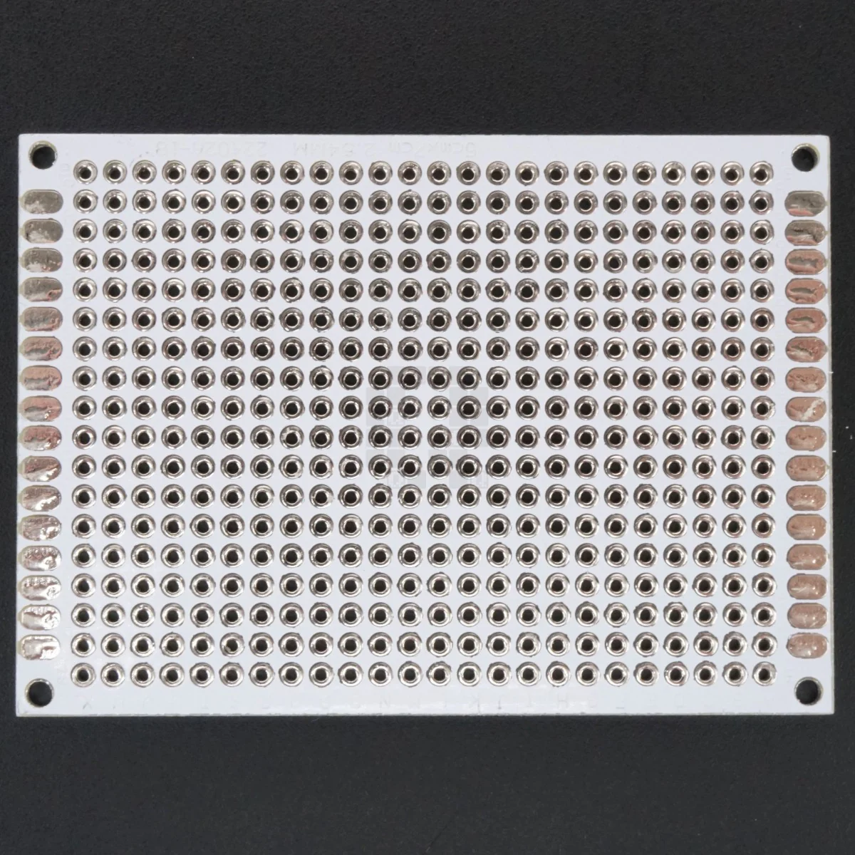
This is the most traditional category, containing no photosensitive components. The pattern is directly printed onto the board via screen printing (the screen itself is the final pattern) and relies entirely on high-temperature baking to cause the resin to undergo thermal polymerization and cure.
- Advantages: The simplest process, extremely low ink cost, and no need for expensive exposure and developing equipment.
- Disadvantages: Extremely low resolution; only applicable to low-end consumer electronics with rough traces and no requirement for solder dams. It is virtually incapable of meeting the demands of modern HDI or server boards.
Among these three types, green has become the "classic color" for solder masks not only because of its visual comfort and high contrast (which facilitates AOI - Automated Optical Inspection) but also because its photosensitive chemical system is the most mature and stable, offering the widest window for exposure parameters.
II. The Two Poles of the Spectrum: The "Inherent Dilemmas" of White and Black Inks
In the colorful array of solder mask options (green, blue, red, black, yellow, white, brown—each available in glossy and matte finishes), white and black are undoubtedly the two extremes with the highest process control difficulty. Their core challenges both stem from a profound contradiction between their extreme optical properties and the chemical reaction requirements of "light curing".
The "Light-Absorbing Black Hole" Effect and Bottom-Layer Curing Challenges of Black Ink
Black is a material that absorbs the full spectrum of visible light. During the exposure process, UV light needs to penetrate the surface layer of the ink to trigger the photoinitiators in the deeper layers to generate free radicals, thereby initiating the polymerization reaction.
- Principle Dilemma: High concentrations of black pigment (usually carbon black or complex black metal oxides) form a powerful "light-absorbing barrier." UV light is intensely absorbed and converted into heat energy within a very short distance of entering the surface layer, causing light intensity to decay exponentially with depth. This results in the surface layer becoming over-cured or even brittle, while the bottom layer (near the copper foil or substrate interface) remains incompletely cured due to "light starvation" (commonly referred to in the industry as "undercured").
- Process Consequences: In subsequent surface treatments such as HASL (Hot Air Solder Leveling), ENIG (Electroless Nickel Immersion Gold), or OSP, the board must endure high temperatures and acid/alkali chemical washes. The poorly cured bottom layer has extremely weak adhesion, making it highly susceptible to "ink peeling" (solder mask peeling) or "pseudo copper exposure". Meanwhile, the surface layer absorbing too much energy can also cause the resin to over-crosslink and shrink, generating micro-cracks.
The "Strong Reflective Mirror" Effect and Energy Dissipation of White Ink
White solder mask is commonly used in LED lighting boards to facilitate uniform light distribution. White ink relies on pigments with a high refractive index (such as titanium dioxide, TiO₂) to achieve a bright white appearance.
- Principle Dilemma: During exposure, the high proportion of TiO₂ particles forms a strong light scattering and reflection network. Most of the incoming UV light is repeatedly scattered and ultimately reflected out of the ink surface, rather than effectively propagating to the deeper layers. In contrast to the "light-blocking" of black ink, white ink suffers from "insufficient light reaching the bottom." A massive amount of exposure energy is inefficiently dissipated, similarly resulting in the bottom-layer photoinitiators failing to initiate adequate polymerization.
- Process Consequences: The outcome is the same as with black ink—poor bottom-layer curing. This makes the white solder mask highly prone to blistering and peeling under the high-temperature shock of hot air solder leveling (HASL). Furthermore, titanium dioxide itself possesses photocatalytic activity, which under certain conditions can accelerate the aging of the surface resin.
III. Coping Strategies and eCloud's Way of Balance
Faced with the process challenges of black and white inks, high-end PCB manufacturers must implement fine-tuned adjustments across materials, process parameters, and inspections:
- Material Formulation Optimization: Utilize specialized models. For example, using special pigments with better light transmittance and photoinitiators with adjusted absorption wavelengths for black ink; for white ink, selecting surface-treated titanium dioxide with lower photocatalytic activity. For high-end boards, a dual mechanism of "UV initiation + thermal curing" is often introduced to compensate for the shortcomings of UV curing.
- Exposure Energy and Film Thickness Management: This is the core of process control. The spectral output of the exposure machine must be precisely set, utilizing energy-incremental or multi-stage exposure strategies. Simultaneously, black and white inks are extremely sensitive to film thickness; the screen printing thickness tolerance must be controlled much more strictly than that of green ink to prevent light attenuation or scattering effects from spiraling out of control.
- Strict Destructive and Non-Destructive Testing: Increase curing degree tests, such as acetone wipe tests, Cross-cut tests to evaluate adhesion, and even utilizing Microsection analysis to directly observe the curing state of the solder mask cross-section.
Professional Commitment from eCloud
Solder mask is not merely the clothing of a PCB; it is the frontline defense for long-term product reliability. Whether you need high-reflectivity LED white aluminum PCBs or high-end black server boards that demand ultimate visual texture and thermal performance, eCloud provides the most stable process support. Our engineering team possesses extensive experience in tuning specialty inks, from precise film thickness control to optimized exposure energy settings, ensuring that pain points like "undercured bottom layers" and "ink peeling" are thoroughly resolved. Feel free to contact eCloud to build the highest quality protective layer for your custom specification projects!
