June 18, 2026
Driven by the continuous evolution of AI servers, silicon photonics modules, and edge computing devices toward higher densities, HDI (High Density Interconnect) boards have shifted from a "high-end option" to the default architecture for many new projects. However, many R&D engineers encounter the same pain point: why does an HDI version of an 8-layer board quote at three times the price of its standard counterpart? In this article, we break down the key design decisions behind HDI costs from a manufacturing perspective.
The manufacturability and cost of any HDI board ultimately come down to these four dimensions:
Key Concept: These four dimensions are never independent decisions. Reducing trace width directly impacts the required layer count, while pad and via sizes will, in turn, dictate your available routing space.
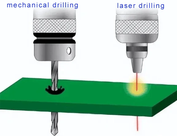
Mechanical drilling is one of the biggest cost drivers in HDI quotes. The unit price of a 6 mil drill bit is significantly higher than a 10 mil one, and the smaller it is, the more fragile and faster it wears out. Mixed‑material stackups also require different drilling parameters, causing the risk of scrap to skyrocket.
In contrast, laser drilling has an often‑overlooked characteristic: the cost difference between drilling 1 hole and 10,000 holes is incredibly minimal. If there are opportunities in your design to replace mechanical through‑holes with laser microvias, prioritise the laser option.
Many manufacturers claim they can achieve a 1:1 ratio, but this is not the optimal working point. Microvias must be electroplated and filled from the bottom up. If the hole is too deep and narrow, it will cause plating voids and a collapse in yield rates.
| Comparison | Staggered Vias | Stacked Vias | | :--- | :--- | :--- | | Process Steps | Fewer (copper filling not required) | More (inner layers must be sealed with copper filling) | | Cost | Low | High |
As long as the vertical distance between the centres of the two vias is greater than the microvia diameter, a staggered design can be used.
Crucial reminder: Never stack a laser microvia directly on top of a “mechanically drilled buried via” – this is a known high‑risk structure in the industry that generates cracks. The accuracy of laser drilling is approximately ±1 mil, so be sure to account for this tolerance during the design phase.
When a design requires Via‑in‑Pad, the board manufacturer must perform additional drilling, via filling, and a secondary plating to cap it. Every time a board returns to a process station, it represents a direct consumption of time and money.
Best Practice: Prioritise using laser microvia + plating shut over mechanical drilling + non‑conductive via filling.
For every additional lamination cycle, the cost jumps to the next bracket:
Finer trace widths and spacing often allow you to complete the same routing with fewer layers. Shrinking from a 4 mil down to a 2 mil line/space might reduce an 8‑layer board to 6 layers. The cost saved from eliminating 2 layers usually far outweighs the unit price increase of using a fine‑line process.
Inner layer fine lines are easier to manufacture than outer layers (as they don’t require heavy copper plating). A 2 mil line/space is already a stable mass‑production standard in the industry, maintaining yield rates above 90%.
When a 0.4 mm or even 0.3 mm pitch BGA appears on the board, HDI is no longer an option but a necessity. Lasers can create smaller pads, freeing up routing space within the BGA area. Inner layers can route 2 signal traces between pads, drastically reducing the overall routing layer count.
When we assist clients with DFM (Design for Manufacturing) preliminary reviews, the most common cost wastes stem from three blind spots:
Bringing the manufacturer into the discussion during the design phase is the most effective way to control HDI costs.
eCloud provides integrated services for complex HDI prototyping and boasts rich experience in high‑speed networking, silicon photonics, edge AI, and RF high‑frequency applications. Planning your next HDI project? Feel free to contact our engineering team to get DFM preliminary review feedback during the layout phase, minimising your cost and yield risks.
