March 13, 2026
In Taiwan's fiercely competitive hardware product development environment, the daily routines of Project Managers (PM) and R&D Engineers (RD) are often filled with countless rounds of specification compromises and cost tug-of-wars. When reviewing the BOM (Bill of Materials), the team's attention typically focuses intensely on the following key areas: ● Procurement prices for the main chip and memory ● Total BOM cost for various passive components ● SMT manufacturing and assembly fees from contract manufacturers However, beyond these obvious expenses, the PCB manufacturing cost structure contains a critical factor that is frequently overlooked by cross-functional teams yet has a decisive impact: PCB panel utilization. This metric not only determines your bare board unit price but also drives manufacturing efficiency in downstream production lines, making it a strategically vital element in DFM (Design for Manufacturability).
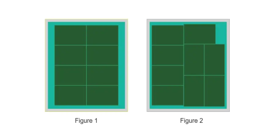
To clarify the impact of panel utilization, we must first demystify the pricing of bare PCBs. In traditional PCB manufacturing, material costs (including FR-4 fiberglass substrate and copper foil) typically account for an absolute 60% to 70% of the total manufacturing cost. This means that when you purchase PCBs from a manufacturer, the vast majority of your money is spent on buying the "material" itself.
When Mechanical Engineers (ME) and Layout Engineers fail to consider this properly during the design phase, resulting in poor panel design and utilization below 70% or even dropping below 65%, the company is effectively paying for large amounts of FR-4 substrate and copper foil that end up being discarded as waste. Imagine buying a whole piece of premium fabric, only to throw 30% to 40% of it directly into the trash due to poor cutting layout. In the thin-margin consumer electronics industry, this is undoubtedly a fatal waste.
More importantly, the damage of low panel utilization is not limited to the procurement cost of bare PCBs; it triggers a chain reaction that severely impacts the performance of downstream assembly plants, including:
This is precisely why, in mature electronics manufacturing companies and top-tier tech firms, panel design is never just an individual task for a Layout engineer, but a core DFM (Design for Manufacturing) issue that must be addressed collaboratively across departments.
Before discussing optimization, we must first establish a precise definition of panel utilization.
Simply put, panel utilization refers to the ratio of the area actually usable for the final product's individual boards (sub-panels) to the total area of a standard PCB production panel.
In the PCB manufacturing industry, factories do not directly produce the small boards you need. Instead, they arrange multiple smaller boards in an array on a standard-sized large panel for lamination, drilling, and plating. The most common standard PCB production panel size in the industry is 18 inches × 24 inches (approximately 457 mm × 610 mm).
Many junior engineers mistakenly believe they can calculate the output quantity simply by dividing the panel area by the individual board area. However, a panel cannot be used "100%" because several indispensable physical spaces must be预留 during the process:
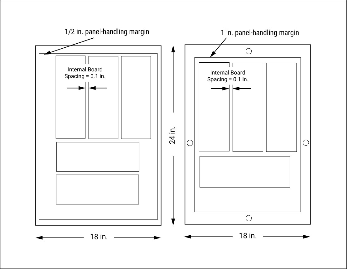 After deducting these "necessary evils," the effective area available for layout is significantly smaller than the theoretical area. In the PCB manufacturing industry, the following standards are commonly used to evaluate the quality of panel layout:
| Panel Utilization | Industry Evaluation Grade | Status Analysis & Recommended Action | | :--- | :--- | :--- | | > 70% | Excellent | Layout is optimized, offering very high cost-effectiveness. | | 50%–70% | Good | Industry norm, acceptable in most applications, but room for fine-tuning. | | 30%–50% | Moderate | Costs start to escalate significantly; strongly consider changing panel size or rotation angle. | | < 30% | Poor | Causes severe material waste; board shape and design must be re-evaluated. |
Data speaks volumes: when utilization falls below 70%, it means over 30% of the laminate ultimately becomes industrial waste. In Taiwan's consumer electronics industry, where gross margins are notoriously thin (often referred to as "3 to 4 percent"), this systemic waste directly erodes the product's net profit, nullifying the hard-won secured by PMs and Sales.
When discussing how to improve utilization, the biggest battleground often lies in the choice of "depanelization technology." In PCB panel design, there are two most common depanelization methods, each with distinct advantages and disadvantages that directly determine the upper limit of panel utilization.
V-cut is a very traditional and efficient depanelization method. Its principle involves using circular blades to pre-cut V-shaped grooves on both the top and bottom sides of the production panel. After the entire panel has completed component placement and reflow soldering on the SMT line, operators or depanelization machines can directly break the individual boards apart along the V-grooves.
Advantages:
Limitations:
Therefore, V-cut is most suitable for PCB designs that are regular rectangles and have a certain thickness.
When the product's mechanical design requires irregular shapes (like a round smartwatch or a uniquely shaped IoT device), or when important connectors on the board edge prevent a straight V-cut, engineers typically use "stamp holes with router depanelization."
This method involves retaining connecting "tabs" between the individual board and the waste border, and drilling a series of small, closely spaced holes in these tabs (resembling the edge of a postage stamp). After SMT assembly, a mechanical router is used to cut through the tabs.
Advantages:
Disadvantages:
These "keep-out zones" reserved for the router bit and stress relief are the primary culprits causing panel utilization to plummet and PCB unit prices to skyrocket.
When reviewing DFM reports, many PMs focus solely on the rising unit price of the bare PCB, overlooking a massive problem hidden deep within the factory: the production efficiency (UPH) of the SMT line.
We must understand that one of the primary purposes of panelization is to配合 the operating logic of SMT machines and improve placement efficiency. Low panel utilization means fewer individual boards can be accommodated on a single large panel. This leads to several致命 impacts:
Furthermore, in the pursuit of极致 utilization, Layout engineers sometimes rotate individual boards by 90 or 180 degrees to fit them into spaces on the panel. While this "Tetris-style" layout improves PCB utilization on paper, it creates another disaster for SMT.
When individual boards on the same panel are oriented inconsistently, the nozzles of the SMT placement machine, after picking up components, must frequently perform microsecond-level "rotation adjustments" to accurately align the components with pads facing different directions. In mass production involving hundreds of thousands of component placements, this significantly reduces overall placement speed.
Therefore, excellent panel design must achieve a perfect balance between " material utilization" and "SMT line efficiency."
In the consumer electronics industry, profits are saved. Real-world精算 data from the industry reveals a惊人的 leverage effect:
For every 1% increase in panel utilization, the manufacturing cost per PCB typically decreases by 1.2% to 1.5%.
Where does this non-linear reduction come from? The reason is that high utilization not only reduces material waste but, more importantly, spreads the fixed process costs (such as exposure, development, plating, lamination, etc.) incurred per panel across a larger number of individual boards.
Let's simulate cost calculation using a realistic project scenario:
Assume the fixed cost for a factory to process one standard PCB panel is $50 USD.
| Cost Comparison Item | Scenario A (Unoptimized Design) | Scenario B (Optimized Design) | | :--- | :--- | :--- | | Number of boards per panel | 80 units | 100 units | | Amortized cost per board | $0.63 | $0.50 |
The table clearly shows that simply by optimizing the layout to increase panel output from 80 to 100 boards, the cost per board drops instantly by 20%.
If the project target is to produce 10,000 PCBA units:
| Mass Production Analysis | Scenario A (Unoptimized Design) | Scenario B (Optimized Design) | | :--- | :--- | :--- | | Panels needed for 10k units | 125 panels | 100 panels | | Total Material & Processing Cost | $6,250 | $5,000 |
Through optimization, the project directly saves $1,250 USD on bare PCB procurement. And this doesn't even account for the additional savings in machine time and efficiency on the SMT line resulting from processing 25 fewer panels (reduced loading/unloading).
Since panel utilization is so critical, how can hardware teams practically reach the 70% or even 85% ceiling? Common and effective optimization methods include the following three:
In the past, engineers mostly relied on experience, slowly drawing grids and calculating layouts using CAD or Excel. Modern advanced PCB factories and R&D teams have already fully adopted professional panelization tools. These types of software have powerful algorithms that can perform Automatic Nesting, including:
They use computer calculations to find the most perfect geometric arrangement while automatically adhering to factory edge clearance and spacing rules. Industry data shows that using such software typically improves utilization by an additional 10%–15% compared to manual layout.
When a single product has an extremely irregular shape (e.g., an L-shaped motherboard) that leaves odd-shaped spaces no matter how it's rotated, the best solution is to mix different PCB designs on the same panel. For example, combine:
All on the same large panel. Use the small module boards to precisely fill the blank spaces around the main board, minimizing waste. For system-level products with multiple sub-boards, this not only saves material but also ensures that one PCBA panel perfectly corresponds to the BOM management for one finished product.
This is the most crucial yet most difficult strategy to execute. The best method is actually quite simple: Consider "panelization" during the very first stages of PCB outline design.
This requires strong cross-departmental collaboration:
In summary, PCB panel utilization is absolutely not just a "factory layout issue" or a trivial matter that can be outsourced to the board house and forgotten. It is actually an engineering decision with far-reaching consequences, directly impacting:
When you receive a DFM report showing panel utilization below 70%, it means the company is essentially paying for a large amount of material that will soon become waste.
Therefore, in a mature hardware development process, teams should adhere to the DFM spirit: evaluate panelization methods early in the design phase, collaborate closely with the PCB manufacturer for layout discussions, and skillfully use automated panelization tools to optimize the matrix. Only by meticulously covering every square inch of FR-4 substrate can tech companies firmly secure their hard-earned profits in the fiercely competitive red ocean of the electronics industry.
