From Tool Selection to PCB Prototyping
Define the task and constraints, then verify electrical requirements and fabrication data.
Describe a requirement, and AI helps select components, connect the circuit, and route the PCB. As the board becomes more complete on screen, exporting Gerbers and ordering prototypes can appear to be the natural next step.
However, “design complete” needs clear acceptance criteria: correct connectivity, suitable footprints, verified electrical requirements, and fabrication files that communicate the intended construction.
When introducing AI PCB design tools, R&D teams should first define the work they want to automate and how they will review the results. These decisions affect tool selection and the engineering effort required afterward.
Tools carrying the AI label can work in different ways. The following three illustrate different approaches; they are not a ranking.
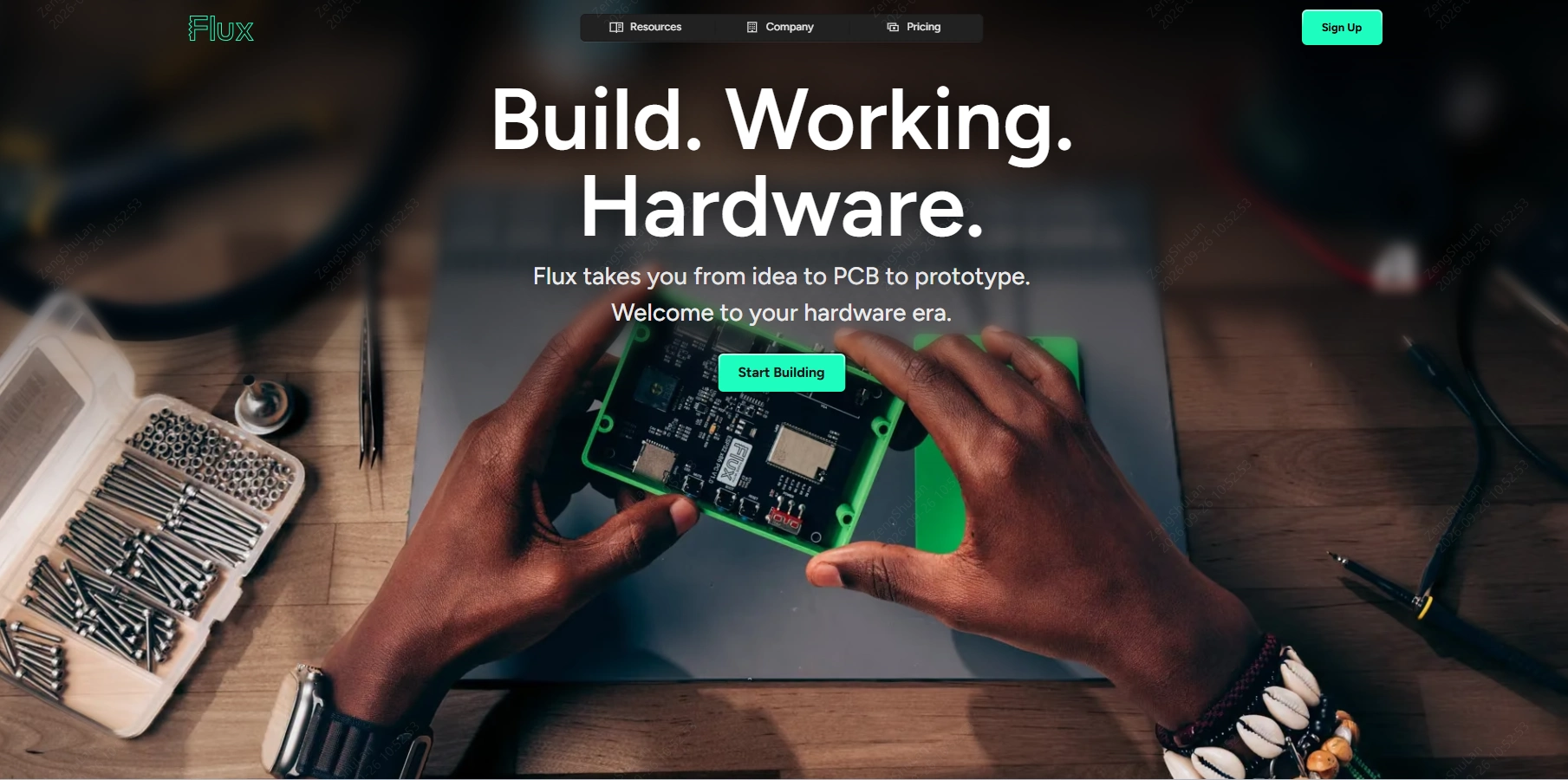 Flux documentation distinguishes Chat and Agent modes. Chat can read projects, explain circuits, and discuss questions. Agent can perform work involving components, connections, PCB setup, and routing.
Evaluate whether the team needs design discussion, targeted changes, or a broader agent workflow, and inspect the actual project after modifications.
Tool documentation: Flux Chat and Agent modes
 Quilter requires an input board file containing an outline, component footprints, and a valid netlist. Inputs can also specify stackups, design rules, and fixed design elements.
The input therefore requires engineering preparation. Connector positions, keepouts, and special routing requirements should be defined before submission, with their handling confirmed.
Tool documentation: Preparing a Quilter input board file
 Allegro X AI provides automation for component placement, power and ground plane creation, and critical-net routing.
For existing Cadence teams, evaluation can focus on integration with current constraints, design data, and analysis workflows, and on identifying suitable tasks for AI.
Tool documentation: Cadence Allegro X Design Platform
Before selecting a tool, answer three questions: What usable data do you have? Where should the tool’s work stop? Can the result be edited and verified in the team’s EDA environment?
“Create a small controller board” can start a discussion, but it is not a complete fabrication specification.
Before automated placement or routing, document:
For example, if a net requires controlled impedance but the project specifies only general trace widths and clearances, completed routing still needs to be checked against the actual stackup. This illustrates constraint preparation; it does not imply that a particular tool will necessarily produce that problem.
Requirements the tool cannot express or verify should be included in a separate engineering review.
What a design rule check, or DRC, can verify depends on tool capabilities, enabled checks, and user-defined rules.
KiCad documentation, for example, describes checks for board rules and unconnected items, with an option to test consistency between the PCB and schematic. Users also need to review ignored checks.
Technical reference: KiCad PCB Editor: Design Rules Checking
When reviewing results, confirm:
Some EDA tools integrate manufacturing rules and analysis capabilities to identify problems earlier. Teams should nevertheless establish which checks were actually performed and which requirements remain unverified.
Verify full part numbers, symbol pins, footprint pins, and manufacturer-recommended lands. Similar names or appearances do not establish that two components are interchangeable.
Check consistency among board thickness, dielectric thickness, copper thickness, and impedance requirements. Through, blind, buried, and other special hole structures must correspond to the actual design and fabrication drawings.
Review solder mask dams and openings around small packages, hole-to-copper spacing, board edges, and mechanical processing requirements. Bare-board fabrication conditions should also be considered alongside assembly needs.
Gerbers, drill files, board outline, fabrication requirements, and impedance tables should come from the same approved revision. For PCBA, also check the BOM, placement files, and assembly drawings.
After export, reopen the manufacturing files in a viewer to inspect layers, alignment, drilling, and outline. Confirm that settings in the native EDA project are reflected in the outputs or accompanying fabrication requirements.
Start evaluation with a board the team understands and for which validation evidence already exists. Apply the same outline, components, and design conditions, then compare results.
Record:
Evaluate the complete workflow rather than measuring only the autorouter’s execution time.
The suitability of an AI PCB design tool ultimately depends on whether it shortens delivery while keeping design conditions and verification results clear and traceable.
For an eCloud prototype inquiry, provide Gerbers, drill files, fabrication requirements, the stackup, and quantities. Identify controlled impedance and special processes to support manufacturing review. The design team should approve functional and electrical verification before fabrication release.