Review copper, cooling and soldering together
Key checks from current-path design to assembly validation.
Increasing copper thickness is a common approach when designing power modules, motor drivers and high-current control boards. However, specifying copper thickness does not complete the review of current paths, fabrication conditions or soldering methods.
High-power PCB design requires electrical requirements, heat-transfer paths and manufacturing conditions to work together. When these are addressed separately, problems may emerge during engineering review or prototype assembly.
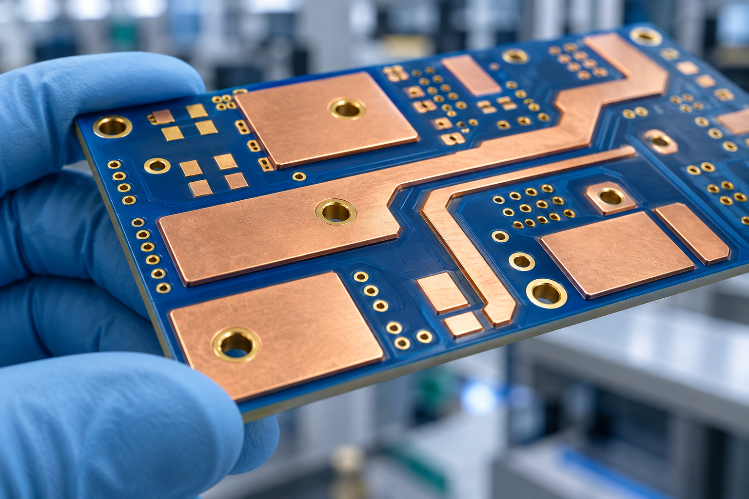 Assess the actual conductor cross-section along the path from the power input through the power components to the output. Narrow connections between copper regions, pad entries and layer transitions deserve individual attention.
Conductor loss depends on current squared and resistance. With the same material and temperature conditions, longer paths and smaller cross-sections increase resistance. Before increasing copper thickness across an entire layer, also consider shortening the path or improving local connections.
For switching power supplies, review the high-current loop and its return path. Heavy copper cannot replace compact component placement and careful loop design.
Technical references: Conductor resistance and losses and power MOSFET layout principles.
 Heavy-copper etching requires consideration of lateral undercut and process compensation. Confirm minimum trace widths and clearances against the fabrication capability for the selected copper thickness, rather than carrying over standard-board design rules.
Fabrication specifications should also distinguish starting copper from finished copper to prevent different interpretations of the delivered outer-layer thickness after plating.
Clearly identify:
The customer defines functional and finished-board requirements, while the fabricator proposes process compensation. Aligning these through engineering queries helps prevent duplicate compensation.
During lamination, prepreg must supply enough resin to fill the spaces between inner-layer conductors. Required resin volume depends on copper thickness, the proportion of copper removed and the target dielectric thickness.
Specifying “1080” or “2116” alone is therefore insufficient to confirm filling conditions. The material system, resin content, number of plies and actual copper distribution also need review.
Discuss resin filling and copper balance together. If the prepreg combination changes, reconfirm the pressed thickness. For impedance-controlled products, also assess the effect of any dielectric-thickness change.
Technical reference: Prepreg selection and dielectric-space assessment.
Thermal vias transfer heat to other copper layers. Thermal-relief connections use narrower copper spokes to restrict heat flow, helping a soldering location reach temperature more easily.
Because their purposes differ, changing every primary heat-transfer connection to thermal relief is not an appropriate general response to difficult soldering.
Evaluate via count, diameter and connection style together. Via count alone does not establish thermal performance.
Technical reference: Thermal vias and thermal relief in motor-driver layouts.
Open vias within a power component’s exposed thermal pad can draw solder into the holes during reflow, affecting the solder volume remaining on the pad. Select the treatment according to the package, via structure and assembly conditions.
Resin filling with copper capping is one option to discuss, but thermal vias beneath components do not all require identical treatment. Drawings should distinguish solder-mask coverage, resin filling and copper capping after filling.
Stencil apertures and solder volume should follow component guidance and be verified through actual builds. For large thermal pads, discuss X-ray inspection and void-acceptance criteria during prototyping. A requirement such as “no voids” needs an executable assessment method.
Technical reference: Thermal-pad, via and assembly design.
A design-for-manufacturing (DFM) review for a high-power PCB should turn open questions into information that can be delivered and checked:
The purpose is to align the designer, fabricator and assembler around the same conditions and give prototype results a clear design basis.
High-power PCB design must answer three questions together: how current flows, how heat leaves and how solder joints form.
Before releasing the design, review current-path bottlenecks, heavy-copper fabrication, prepreg filling and vias within pads. Then plan corresponding prototype verification so that any revisions have a concrete basis.
For projects involving heavy copper, high current or power-component assembly, provide the Gerber files, proposed stackup, finished copper thickness by layer and critical component information to discuss fabrication requirements and open questions with eCloud.
