Optical Transceivers from 800G to 1.6T
Review materials, vias, and card-edge contacts before committing to an optical transceiver PCB prototype.
The impedance report passes, and the laminate is a low-loss grade. Yet the assembled product still cannot pass high-speed testing consistently.
For optical transceiver development teams, troubleshooting is difficult because materials, routing, packaging, and fabrication variation may all contribute. Moving to a more expensive laminate may leave the actual bottleneck unresolved.
As modules advance from 800G to 1.6T, optical transceiver PCB design must consider impedance, loss, interconnect structures, and thermal management together.
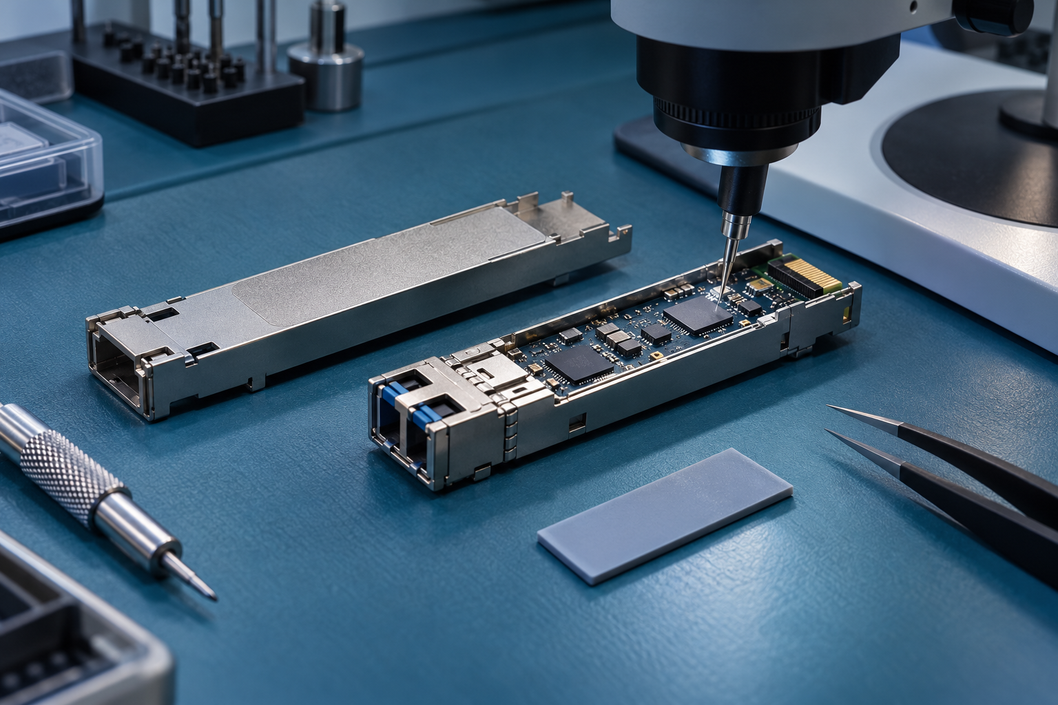
An optical transceiver converts electrical signals into optical signals and vice versa. Its PCB provides electrical interconnections, power distribution, and control.
In a pluggable module, card-edge contacts connect to the host. Depending on the architecture, circuitry on the board connects signal-processing, driver, receiver, and optoelectronic components. Optical assemblies can use different packaging approaches; a TOSA/ROSA arrangement should not be assumed for every product.
The PCB also participates in heat transfer. Heat removal, however, depends on chip-to-case contact, thermal interface materials, and system cooling. Establish the actual thermal path before increasing copper thickness or adding thermal vias.
800G and 1.6T describe aggregate module capacity. Layout decisions also depend on the number of electrical lanes and the data rate per lane.
Typical OSFP configurations include eight 100G electrical lanes for 800G and eight 200G lanes for 1.6T. OSFP MSA overview
Electrical and optical interfaces do not necessarily use identical lane configurations. Review the host interface, internal module interconnects, and optical architecture separately to avoid confusing rates at different points.
Consequently, a “1.6T” designation alone cannot establish the required layer count, trace width and spacing, or need for modified semi-additive processing (mSAP). These depend on package pitch, escape-routing space, channel paths, and manufacturability.
Impedance control helps manage the geometric and electrical consistency of transmission lines. Channel performance also includes insertion loss, reflections, and crosstalk.
Even when straight transmission-line sections meet impedance requirements, transitions through pads, AC-coupling capacitors, vias, and card-edge contacts can introduce local discontinuities.
Unused via stubs can also affect high-speed signals. Channel analysis should determine whether to address them through routing-layer selection, blind vias, or backdrilling, with fabrication tolerances confirmed. Via and signal-integrity design guidance
Before prototyping, distinguish the purposes of each verification activity:
An impedance coupon provides valuable evidence, but it cannot directly replace validation of the complete product channel.
Dielectric constant, Dk, affects propagation and impedance. Dissipation factor, Df, relates to dielectric loss. Material selection must account for test frequency, measurement method, and the material construction represented by the values.
A datasheet Dk value should not automatically become a simulation input. Material suppliers provide Design Dk as a reference for circuit design and modeling, but its applicable conditions still require confirmation. Dk and Design Dk explained
Copper foil is another frequently overlooked variable. The same material name can produce different losses when combined with different copper foils and trace dimensions. Material, copper, and insertion-loss reference
Prototype specifications should therefore identify the complete material designation, dielectric thickness, copper foil type, and finished copper thickness. Any material substitution should trigger a review of the stackup, impedance, and loss model, followed by approval.
Fine traces help with dense escape routing, but high-speed routing must also account for conductor loss and dimensional variation. Apply minimum trace width and spacing according to local needs rather than extending escape-region dimensions along an entire high-speed path.
During design-for-manufacturing discussions, confirm:
Producing one prototype and maintaining consistency across subsequent batches require separate assessments.
Card-edge contacts involve mating durability, plating, board geometry, and contact position. Specifying only a “gold finish” leaves essential requirements undefined.
The OSFP MSA, for example, addresses card-edge interfaces and contact plating separately. Fabrication requirements should follow the selected specification revision, connector, and product conditions. Mating contacts and assembly pads also need to be distinguished when specifying surface finishes. OSFP module specification
Thermal review should follow heat from the main dissipating components to the case and heatsink, while checking thermal-pad contact, assembly height, and board warpage. PCB revisions that change component height or local stiffness should also trigger a mechanical-fit review.
 Effective optical transceiver PCB design translates electrical requirements into conditions that can be manufactured, measured, and traced. Beyond the material grade, development teams need to understand whether each material or process change alters the original channel assumptions.
For an optical transceiver PCB prototype, provide Gerber data, the stackup, impedance requirements, and mechanical constraints to discuss engineering pre-review and fabrication conditions with eCloud. Specialized fine-line processes and validation activities should be assessed for feasibility and scope on a project basis.