Subtractive × mSAP × SAP
Understand base copper, pattern plating, and etching before choosing a high-density PCB process.
As BGA pitches shrink and component density increases, layout engineers face a practical problem: the existing line and space rules no longer allow signals to escape.
mSAP and SAP often enter the discussion at this point. Their differences, however, extend beyond minimum feature size. They form copper circuits differently and require different amounts of copper to be removed during fabrication.
Understanding these differences helps engineers decide when a process upgrade is justified—and prevents a supplier’s demonstrated limit from becoming an assumed production design rule.
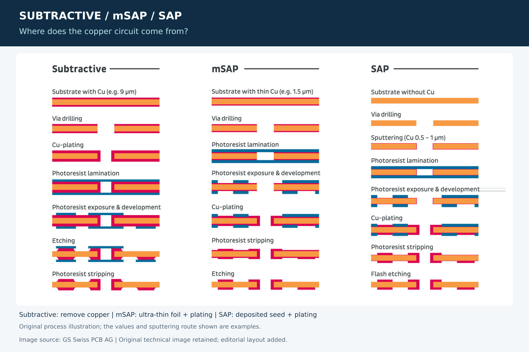
A subtractive process starts with copper and removes the unwanted material.
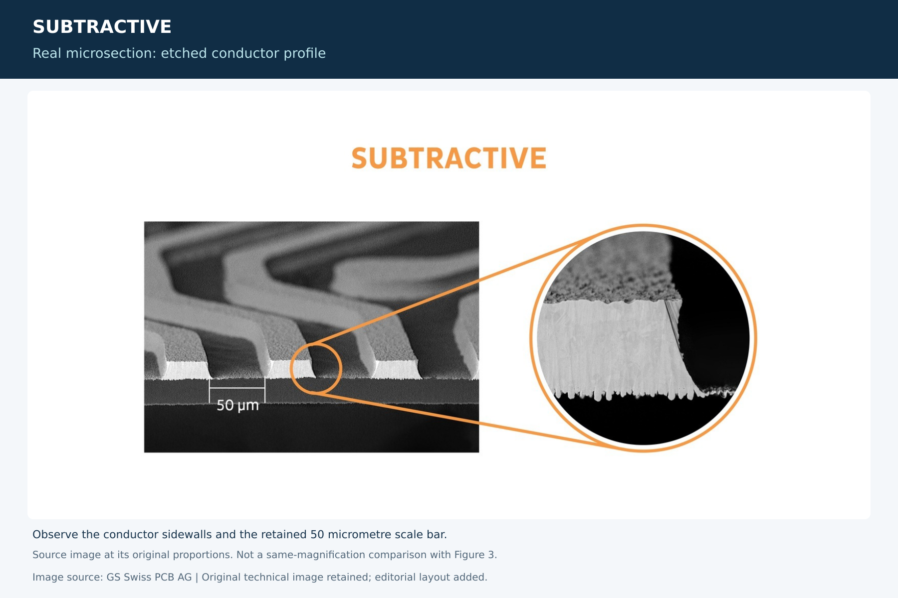 A simplified circuit-formation sequence is:
Actual inner- and outer-layer processes may use different plating and resist arrangements, but the circuit is primarily defined by copper etching.
Etching removes copper laterally as well as vertically. As the copper to be removed becomes thicker, controlling fine circuit dimensions generally becomes more difficult.
Consequently, 50–75 μm should not be treated as an absolute lower limit for subtractive processing. Thin copper and process optimization can support finer patterns. The relevant question is what line and space the fabricator can consistently deliver at the specified finished copper thickness.
The modified semi-additive process, or mSAP, changes the main circuit-formation step:
Photoresist defines the circuit openings, and pattern plating builds most of the conductor thickness.
A simplified sequence is:
Because less base copper must be removed, etching can have a smaller effect on finished circuit dimensions.
Ultra-thin foil is not universally limited to 2–3 μm. For example, Mitsui Kinzoku’s published MicroThin range includes 1.5–5 μm foil. This is a material product range, not a statement that every mSAP line uses the same starting conditions.
mSAP does not eliminate etching risks. Insufficient flash etching can leave copper that causes shorts; excessive etching can reduce conductor width and thickness. Fine patterns also require control of imaging, plating uniformity, and resist removal.
SAP stands for semi-additive process, not fully additive process.
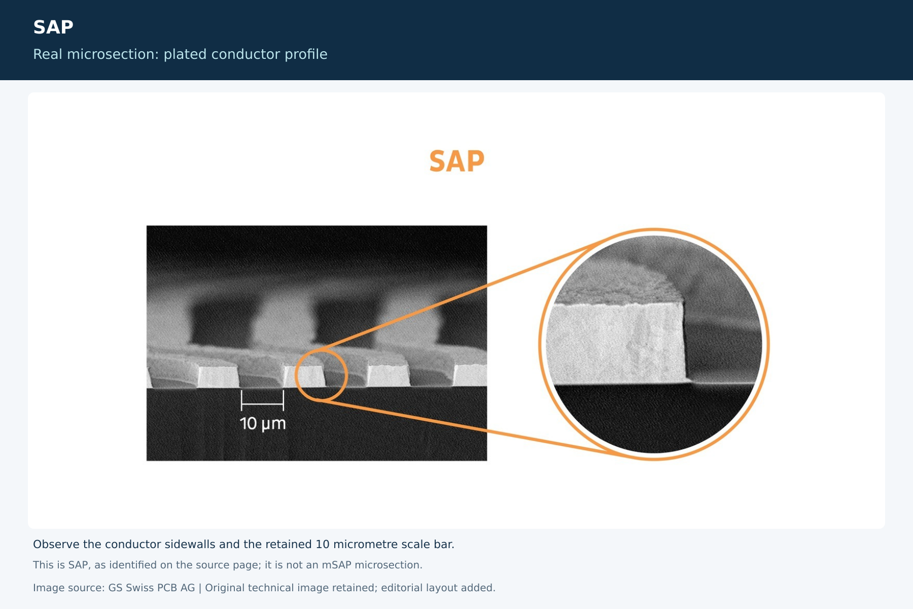 Both SAP and mSAP use pattern plating. A key distinction is the source of the underlying conductive layer:
SAP seed layers may be formed by electroless deposition. Some technology routes use sputtering and associated adhesion layers. After circuit plating, the exposed seed between conductors must still be removed.
A thinner seed supports further feature reduction, while making dielectric preparation, adhesion, and process integration especially important.
SAP supports finer patterns, but it should not be defined as “normally below 5 μm.” For example, PCB Technologies publicly describes SAP capability reaching 5 μm line and space. That is a specific technology capability, not a universal supplier specification.
Three starting points capture the essential differences:

 Suppliers may also use classifications such as amSAP. Process names explain the general route, but they cannot replace a complete manufacturing specification.
HDI, SLP, BT, and ABF are also not four mutually exclusive circuit-formation methods.
HDI describes high-density interconnect structures. SLP describes a substrate-like PCB product concept. BT and ABF relate to material systems. Product structure, materials, and circuit formation should therefore be discussed separately. A smartphone SLP motherboard and a memory package substrate should not be treated as the same product category.
mSAP supports denser circuit layouts and is closely associated with miniaturized electronics such as smartphones. Smartphone motherboards and IC package substrates nevertheless serve different assembly functions and manufacturing requirements.
A 0.35 mm BGA pitch does not, by itself, establish a requirement for 20–25 μm routing.
The requirement also depends on pad diameter, ball arrangement, microvia pads, available routing layers, and clearances. Engineers should identify the constrained escape channels before evaluating a semi-additive process.
Local fine-line routing also does not mean that an entire high-speed channel should use the same narrow width. Outside the dense area, routing must still address impedance and loss requirements.
High-speed optical modules are a real application for mSAP, but “all 1.6T modules require 15/15 μm” is not an appropriate general rule.
For example, AT&S publishes optical transceiver product data covering 400G through 1.6T, with mSAP line and space down to 18/22 μm. This is an identified supplier’s capability, not a common specification for every optical module.
Similarly, a 7-2-7 stackup and approximately 1 mm board thickness must be tied to a particular design. They cannot be determined from data rate alone.
For emerging architectures such as CoWoP and NPO, obtain the interconnect interface, package arrangement, and qualification conditions before selecting a PCB process. An architecture name alone does not establish a 15–20 μm routing requirement.
Likewise, operation at 77 GHz does not automatically require mSAP. Materials, copper roughness, dielectric thickness, conductor geometry, and surface finish all influence millimeter-wave performance.
 A more rectangular conductor profile supports dimensional control, but it does not automatically guarantee ±3% or ±5% impedance. Impedance must still be evaluated using dielectric thickness, Dk, finished copper thickness, and actual conductor dimensions.
Cost should also be compared at board level rather than through a fixed multiplier. Finer routing may change layer count or board area, but determining whether those changes offset additional process cost requires an actual design and quotation.
Choosing between subtractive processing, mSAP, and SAP requires a combined assessment of manufacturability, electrical requirements, and cost.
For R&D teams, the priority is to identify where fine routing is actually needed and confirm materials, copper thickness, stackup, and qualification conditions together.
When evaluating a high-density PCB prototype, provide eCloud with the Gerber files, BGA package information, proposed stackup, and critical specifications. Clarifying the manufacturing requirements first supports selection of an appropriate supply solution.